AI Transforms the EDA Industry: Will the Top Three Players Be Reshuffled?
 05/06 2025
 850
850
Preface:
Analysts at the China Chamber of Commerce Industry Research Institute predict that by 2025, China's AI chip market will reach a size of 153 billion yuan, with ample room for growth in the EDA+AI sector.
In the golden era of AI chips, EDA+AI is not merely a technical tool but a strategic asset.
Author | Fang Wensan
Image Source | Network
EDA Technology Reaches the Limits of Traditional Approaches
As chip sizes continue to expand, reaching billions or even trillions of logic gates, traditional methods struggle to manage increasing complexity, especially with heterogeneous architectures and shortened development cycles.
This presents an opportunity for new tools and methods. For instance, AI agents can be integrated into existing EDA tools, enhancing functionality rather than replacing the existing tool chain. From specification generation to RTL code and test platforms, AI agents interpret waveform outputs, debug traces, and provide adaptive suggestions based on internal codebases and naming conventions.
The future of EDA productivity lies not just in higher-level languages or new verification frameworks but in AI agents collaborating with engineers, offering guidance, enhancements, and acceleration through domain-specific intelligence.
This goes beyond automating routine tasks; it helps engineers gain deeper problem insights, access relevant context, and make architectural trade-off decisions faster and with greater confidence.
To achieve true scalability at the trillion-gate level, the EDA industry must transcend scripts and templates, building intelligent systems that autonomously integrate codebases, historical designs, and evolving specification contexts.
EDA Sub-sectors Undergo Profound AI-Driven Changes
Developments in large models like DeepSeek are increasingly demonstrating their pivotal role in the EDA industry.
AI technology optimizes the chip design process through machine learning algorithms, enhancing design efficiency and accuracy. For example, AI algorithms can be applied to EDA tool stages such as simulation and verification, placement, and routing, accelerating the design process and reducing errors.
Currently, the integration of AI technology and industrial software is gradually permeating all aspects of integrated circuit design, manufacturing, packaging, and testing.
In EDA, there is a mutually beneficial relationship between EDA and AI. During integrated circuit design and production, EDA tools integrated with AI algorithms can more intelligently process complex data, optimize placement and routing, and accelerate simulation and verification. Simultaneously, EDA tools provide high-precision and efficient design solutions, enhancing AI chips' performance in key metrics like computing power and energy efficiency ratio.
Against the backdrop of continuous innovation and evolution in application scenarios, large AI models have continuously evolved from basic to general and industry capabilities.
Meanwhile, intelligent devices such as robots and connected vehicles are also making significant progress, accelerating the release of new productive forces' potential.
According to expert predictions, large AI models will be implemented in core scenarios across more than half of industries, with global demand for AI computing power expected to increase by over 500 times by 2030.
Currently, smart computing chips increasingly demand high-performance, high-precision computing, high energy efficiency ratio, high memory bandwidth, and high interconnect bus bandwidth, while also placing higher demands on large-scale design and advanced packaging technology.
To address challenges posed by technological divergence and break through limitations in computing power, storage, energy consumption, and interconnectivity, the entire chip industry chain, particularly the independent research and development and localization of EDA and IP basic tools, has become indispensable.
The application of AI in EDA is gradually emerging, bringing new breakthroughs to chip design. AI technology can be applied to circuit optimization, fault diagnosis, placement, and routing, improving design quality and shortening the R&D cycle.
Some advanced EDA tools use deep learning algorithms to predict circuit performance, assisting designers in finding the optimal design solution faster. By learning vast amounts of historical design data, AI can automatically generate optimized circuit layouts, reducing manual design workload and error rates.
Additionally, the development of open-source EDA tools has injected new vitality into the market. With the increasing maturity of open-source projects like OpenROAD and Yosys, designers now have more choices.
According to market analysis, the global market size for open-source EDA tools is estimated to reach $100 million by 2023, with expectations of doubling by 2025.
The rise of open-source EDA tools not only lowers the design threshold but also promotes global innovation in EDA technology. For instance, Google's TensorFlow Lite for EDA project, leveraging AI to accelerate the chip design process, points to a new direction for open-source EDA tool development.
The open-source community's collaboration mode encourages global developers to jointly participate in EDA tool development and optimization, accelerating technological progress.
Global EDA Leaders Embrace AI
In close collaboration with Renesas Electronics, Cadence Design successfully developed an AI-based solution integrating Cadence's Verisium Platform and Xcelium ML App. With Xcelium App's machine learning technology, Renesas Electronics' verification team can generate more streamlined regression results.
The Verisium AI-driven application significantly improves Renesas Electronics' overall debugging efficiency, reaching six times the original level and effectively shortening the verification cycle.
Synopsys has launched Synopsys.ai, a tool integrating collaborative, generative, and autonomous functions through conversational intelligence. Thanks to LLM support, Synopsys.ai's generative AI function can be used in both local and cloud environments.
In Siemens' EDA solutions, AI technology is primarily applied in three key areas: core technology, process optimization, and providing a scalable open platform. For instance, in design, AI can deeply analyze and help identify problem root causes while preventing potential future issues.
These capabilities are crucial for automating and validating AI-derived results. By the end of 2024, Siemens acquired the EDA company Altair for $10.6 billion, combining Siemens' online digital platform Xcelerator with Altair to build the world's most comprehensive AI design and simulation product portfolio.
AI Empowers Domestic EDA Enterprises
With the continuous development of AI technology and increasing demand for high-performance computing capabilities, EDA software, as a crucial auxiliary tool for enhancing algorithm efficiency, has become increasingly important.
Against this backdrop, the strategic layout of EDA enterprises is evolving, with global EDA players demonstrating this trend. In February this year, Gridless announced that its SemiMind platform integrated DeepSeek, achieving three core functions:
- Integrating industry expertise and extensive process data to build a domain knowledge base.
- Supporting users in quickly building customized functional modules through low-code/no-code methods.
- Intelligently upgrading the data analysis software platform to provide personalized recommendations, automated process management, and real-time data analysis.
Also in February, domestic FPGA chip design EDA software eLinx announced its integration with DeepSeek, supporting rapid FPGA functional module generation, precise code syntax and logic error identification, and code performance improvement.
Technical trends indicate that the integration of cloud computing, AI, and EDA has become a significant trend in current EDA technology development. Many EDA vendors have launched cloud-based solutions to reduce user costs and enhance design efficiency.
Domestically, HuaDa Nine Skies has developed the ICExplorer-XTop® timing and power optimization tool and the Empyrean Skipper® layout integration and analysis tool to meet AI chip design needs.
Gridless's INFINITY-AI system is an open machine learning platform for the semiconductor manufacturing industry, covering applications like automatic defect classification (ADC) and wafer map defect pattern analysis (WPA). It supports one-click operations for data management, model training, evaluation, and deployment.
CoreSemi's 3DIC Chiplet solution provides a comprehensive Chiplet design solution, including 3DIC design, SI/PI/multi-physics field analysis. The platform employs AI-driven mesh segmentation technology, cloud computing-powered distributed parallel computing, and a joint simulation engine supporting bare chips, interposer layers, and substrates.
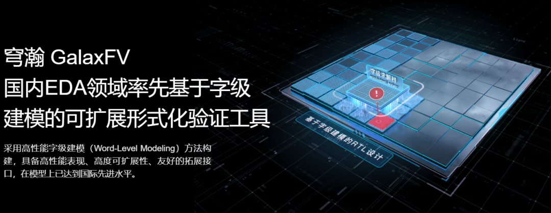
ChipNova offers an AI chip verification and debugging solution to improve AI chip verification efficiency. Its formal verification tool GalaxFV can be combined with simulation technology to accelerate AI verification coverage convergence. The intelligent scenario verification tool GalaxPSS can automatically generate cross-platform, reusable, and intelligent self-regression test stimuli using scenario modeling. The digital verification debugging system Fusion Debug runs across all tools, providing a cross-platform efficient debugging solution.
The Key to Deep EDA-AI Integration: Generative AI
In the EDA industry, AI's application is more about enhancing existing tools rather than replacing designers. Generative AI needs to be data-driven, but the EDA field's business environment hinders data free flow.
Currently, generative AI's primary application in EDA focuses on the automatic generation of design assets. PCB design is time-consuming and complex, and generative AI is seeking breakthroughs in this area. Engineers typically extract information from product specifications to generate design assets like symbols and 3D models. If AI can handle these tasks, product time-to-market will significantly shorten.
EDA industry data is diverse, encompassing both traditional textual information and vast amounts of complex graphical data. Handling this multimodal data is crucial for deeper generative AI integration into the EDA process.
Notably, there's a unique contradiction between the EDA industry and generative AI. EDA is highly data-sensitive, and many semiconductor companies impose strict confidentiality measures on their design and verification data, limiting AI development.
This year, under the dual pressure of international technology blockades and rapid market demand iteration, the domestic EDA industry has shown structural changes. Traditional enterprises are accelerating technology stack and industrial integration upgrades, while emerging enterprises are opening new battlegrounds in AI-driven design and cloud-native EDA.
AI is profoundly transforming the EDA industry. Due to EDA's extremely high accuracy requirements, the corresponding cost of trial and error is also very high. Without substantial industry data accumulation, reliable support cannot be provided. Therefore, the commercialization path for EDA and AI integration still requires time.

Conclusion:
While all EDA enterprises are exploring AI technology to solve practical problems, AI's innovative impact on EDA tools has yet to reach a disruptive level.
Facing international giants' ecosystem advantages, domestic EDA vendors are striving to occupy a place in the global semiconductor design tools market by adopting AI technology and closely linking with the market. However, this battle is far from over, and the next three years may become a critical period for testing the effectiveness of domestic EDA enterprises' differentiation strategies.
Some References:
- STAR Market Daily: "Unicorn ChipNova: AI Becomes the Breakthrough for the Next Generation of EDA"
- eCompany: "Domestic EDA M&A Integration Surge! Helping Enterprises Build Full-Spectrum and Full-Process Capabilities"
- Global Semiconductor Watch: "Domestic EDA, The Path to the Future?"
- Guangming Net: "HJTS: A Breakthrough Sample of China's New Productive Forces in the Era of AI Computing Power"
- Chip Flow Technology Review: "The Invisible Battlefield of AI Chip Design, Domestic EDA is Undergoing a New Round of [Revolution]"
- China Electronics News: "AI is Coming, How will EDA Evolve?"
The Semiconductor Industry Landscape: "Can DeepSeek Spark a Revolution in EDA? Exploring the Changes and Constants"
Kun Shao Reveals: "Exclusive Interview: Industry Pioneers from Cadence, Siemens, and Keysight Delve into the Generative AI-Driven Transformation of EDA"
-
![]()
Model Giant Jieyue Xingchen Steps into Smartphone Arena: A Strategic Alliance with Huaqin Technology
-
![]()
Big Model Firm Dives into Phone Market: StepFun and Wingtech Forge a ‘Dynamic Duo’
-
![]()
Zhongrun Optics Makes a Bold Move with 1 Billion Yuan Investment: Is a Turning Point on the Horizon for the Precision Optics Industry?
-
![]()
Deploy CLBO Crystals and YIG Single Crystals! Erythritol Leader Invests 30 Million in Youwei Optoelectronics
-
CXMT’s July 16 Subscription: Leading Domestic Memory Manufacturer—What’s the Earning Potential per Lot?
-
![]()
Rhythm Discrepancy and Premium Value Erosion: Foreign Luxury Brands Must Re-evaluate Their China Strategy
-
![]()
Half-Year, 1 Billion Yuan Financing, 7 Billion Yuan Valuation: A New Dark Horse Emerges in the Embodied AI Sector
-
![]()
Strong Rebound for Tech Stocks in Hong Kong Stock Market: Is It Time to Bottom-Fish?