DRAM Chips: The Optimal Window Has Arrived
 05/15 2025
 903
903
In April, the memory chip industry seemed to reach a pivotal turning point.
Early in the month, I reported on price hikes by companies like SanDisk and Micron. By month's end, market research data summarized the month's memory chip price trends.
According to DRAMeXchange data on April 30, the fixed transaction price of DDR4 8Gb (gigabytes) products used in personal computers was $1.65, an increase of 22.22% from March. The fixed transaction price of 128Gb MLC NAND flash memory used in memory cards and USBs also increased by 11.06% from March, reaching $2.79.
The primary reason for these price fluctuations is that IT equipment manufacturers are eager to increase chip inventory to mitigate US tariff risks, thereby driving procurement demand.
From the current market perspective, if you ask when the optimal window for memory chips will arrive, I believe it has already opened.
In just one week, there were two price increase announcements in the DRAM market, from SK Hynix and Samsung Electronics.
Recently, supply chain sources revealed that SK Hynix has adjusted prices for its consumer-grade DRAM chips, with an increase of over 10%. Another report stated that SK Hynix plans to raise DDR5 DRAM prices by 15%-20%.
At the beginning of May, Samsung Electronics reached an agreement with major customers to increase the selling price of DRAM chips. DDR4 DRAM prices increased by an average of 20%, and DDR5 DRAM prices increased by approximately 5%. Samsung Electronics has signed DRAM supply contracts with customers at these increased prices and stated that DRAM prices across the entire semiconductor industry are rising. This is the first time Samsung Electronics has raised DRAM prices this year and the first time in nearly a year.
Industry insiders said that although the semiconductor market faced the challenge of oversupply last year, market supply has shrunk as major producers have reduced output. Currently, with Samsung initiating price increases, a new round of contract negotiations is underway.
However, price increases are just one aspect of the current DRAM market performance. Changes in this market do not stop here.
One of the most notable changes is the competitive landscape of the DRAM market.
In February this year, market sources reported that major DRAM manufacturers such as Samsung, SK Hynix, and Micron plan to terminate production of DDR3 and DDR4 memory in the second half of 2025. This decision is driven by the increasing demand for the latest memory technologies such as HBM (High Bandwidth Memory) and DDR5, as well as the decline in profitability of DDR3 and DDR4 memory.
It is expected that starting from summer 2025, due to the withdrawal of these major manufacturers, the supply of DDR3 and DDR4 on the market will significantly decrease, potentially leading to actual supply shortages.
Specifically, SK Hynix stopped supplying DDR3 at the end of 2023 and reduced the production proportion of DDR4 to 30% in the third quarter of 2024, further reducing it to 20% in the fourth quarter. Samsung stopped producing DDR3 in the second quarter of 2024 and continued to reduce DDR4 capacity, shifting towards high-end products such as DDR5 and LPDDR5.
In addition, Nanya Technology, Taiwan's largest DRAM chip manufacturer, is also shifting its main production capacity to DDR4 and DDR5, with DDR3 only accepting customer foundry orders.
However, from the current market situation, it seems that the chip giants' DDR4 production reduction may not be too swift. After all, these companies are gradually increasing product prices in recent days, which also proves from another aspect that the current market demand for DDR4 is relatively strong.
In the field of DDR5 and HBM, domestic storage companies have limited competitiveness, but as international manufacturers gradually withdraw from the DDR3 and DDR4 markets, domestic storage is expected to take over this part of the market demand with cost advantages.
DDR3 is primarily used in consumer electronics and network communications fields such as LCD TVs, digital set-top boxes, WiFi routers, sweeping robots, and network switches. Focusing on the domestic industrial chain, China's DDR3 product performance is on par with overseas manufacturers, with fabless manufacturers such as GigaDevice, Beijing Innochip, and Dongxin Semiconductor mainly focusing on DDR3 and low-capacity DDR4.
According to recent statistical reports released by various research institutions, they all indicate that in the battle for DRAM market share between SK Hynix and Samsung, SK Hynix topped the list for the first time, ending Samsung's market dominance of over 40 years.
According to the DRAM memory market share report for the first quarter of 2025 released by industry research firm Counterpoint, SK Hynix surpassed Samsung Electronics for the first time in that quarter, occupying the top position in the market. This achievement is primarily attributed to its outstanding performance in the HBM field.
Data shows that in the first quarter of 2025, the world's three major DRAM vendors - SK Hynix, Samsung Electronics, and Micron Technology - occupied market shares of 36%, 34%, and 25%, respectively, with the remaining 5% shared by other vendors. In the HBM market segment, SK Hynix holds a dominant position of 70%.
Subsequently, CFM also released statistical data. Driven by the demand for AI servers and the recovery of PC and mobile demand, coupled with the impact of some restocking demand triggered by tariffs, the overall performance of DRAM in the first quarter of 2025 was better than expected. The global DRAM market size increased by 42.5% year-on-year to $26.729 billion, with a decrease of 8.5% quarter-on-quarter. During this period, SK Hynix topped the global DRAM market for the first time with a market share of 36.7% due to its absolute advantage in the HBM field.
The smoke of the throne change has not yet dissipated, and the storage track has already sparked an even more intense technological rivalry.
To overcome DRAM scaling limitations in advance and lead the next generation of memory manufacturing, several technology giants are continuously developing new memory technologies, hoping to take the lead in the upcoming storage competition.
DRAM, Entering the EUV Era
First, let's examine the current state of competition among the three major memory chip giants at advanced process nodes.
Since 2016, DRAM has been hovering at the 10nm level (19nm to 10nm, or 1X), and the three major memory vendors (Samsung, SK Hynix, and Micron) have also launched multiple generations of processes.
Each upgrade involves reducing the size of DRAM cells in certain dimensions to achieve increased density and reduced power consumption.
The naming conventions for processes in the storage industry are unique and called: 1x, 1y, 1z, etc. The 1X nm node is between 16-19nm, 1Y nm is between 14-16nm, and 1Z is approximately 12 to 14nm.
1α is an evolution of the DRAM process after 1z. According to current information, the 1α manufacturing process roughly corresponds to a 10-12nm process. 1α-nm may correspond to a smaller 12~14nm, 1β-nm may correspond to 10~12nm, and 1γ-nm may correspond to 10nm.
Currently, this technological competition has reached 10nm and below.
According to Korean media ETNews, in response to the dual challenges of yield and performance for its 12nm-class DRAM memory products, Samsung Electronics has decided to redesign the new version of 1b nm DRAM while improving the existing 1b nm process. This project is named D1B-P. At the same time, they have adjusted the development plan for the sixth-generation 10nm-class (1C) DRAM.
On the other hand, the development progress of Samsung Electronics' sixth-generation 10nm-class 1c DRAM process has been delayed. Originally, it was planned to increase the yield of 1c nm process DRAM to 70% by December 2024, reaching the level required to end development work and enter mass production. However, in reality, although Samsung successfully produced good grains of 1c nm DRAM at the end of 2023, the overall yield could not meet the requirements. According to market sources, Samsung plans to increase the yield to about 70% within the next six months.
Samsung's previous generation 1b nm memory was developed in October 2022 and mass-produced in May 2023. According to the new plan, the development of 1c DRAM is scheduled to end in mid-2025, and mass production may be delayed until the end of 2025. The interval between the two generations of DRAM processes will be about 2.5 years, which is significantly longer than the industry's general development cycle of 1.5 years.
Samsung's competitor SK Hynix announced the completion of 1c DRAM development at the end of August 2024 and plans to start mass-producing 1c nm DRAM chips in February 2025, becoming the world's first memory supplier to use 1c nm process to produce DRAM chips.
In February this year, Micron announced that the company has delivered the first DDR5 memory samples of the 1γ (1-gamma), sixth-generation (10nm-class) DRAM node designed for next-generation CPUs to ecosystem partners and specific customers. This milestone of 1γ DRAM builds on Micron's previous leadership in the 1α (1-alpha) and 1β (1-beta) DRAM nodes, aiming to provide innovations that support future computing platforms, from cloud to industrial and consumer applications, to edge AI devices such as AI PCs, smartphones, and automobiles.
In the process of advancing technological iteration, EUV has attracted attention from all parties.
According to SK Hynix, the semiconductor industry has been preparing to realize the 10nm-scale process with EUV lithography machines. By utilizing light with a wavelength of 13.5nm, EUV lithography machines achieve finer semiconductor circuit patterns than existing 193nm ArF without requiring multiple patterning. This method reduces the number of processing steps, resulting in a shorter manufacturing time than current multiple patterning technologies (such as Quadruple Patterning Technology, QPT), making EUV the only breakthrough so far.
As early as 2020, memory chip giants had already noticed the convenience of EUV in future advanced process manufacturing.
Samsung was the first among the three major memory manufacturers to introduce EUV. In March 2020, Samsung announced the use of EUV lithography equipment to manufacture 10nm DRAM chips and delivered 1 million 10nm-class (D1x) DDR4 DRAM modules based on EUV technology in the same year. In October 2021, Samsung officially mass-produced 14nm EUV DDR5 DRAM.
It is reported that to stabilize the EUV process, Samsung has not only deployed more than 30 EUV devices (the largest scale globally) but also established a special working group led by former Intel expert Lee Sang-hoon to oversee photoresist material development and light source optimization. Internal data shows that by improving the mask protective film and defect detection algorithm, the recent EUV layer yield has been increased to over 85%.
In addition, Samsung Electronics plans to install the first High-NA EUV (extreme ultraviolet lithography) lithography machine from ASML in its Hwaseong campus.
In February 2021, SK Hynix completed the first EUV fab M16 for DRAM, officially introducing EUV lithography equipment, and announced the mass production of 8 gigabyte LPDDR4 EUV DRAM with the 1a nm process in July of the same year.
SK Hynix adopts a gradual expansion approach, cooperating with the US company Applied Materials to develop a hybrid lithography solution in an attempt to balance cost and performance. It adopts a more conservative strategy. Although it plans to apply more than five layers of EUV processes in D1c DRAM. It is reported that more than 10 EUV lithography machines are currently operating at the M16 factory in Icheon. In last year's organizational adjustment, SK Hynix disbanded its originally independently operating EUV technology team and incorporated it into the Future Technology Research Institute. This adjustment demonstrates SK Hynix's determination to focus on long-term technological breakthroughs rather than merely pursuing short-term production increases.
In SK Hynix's plans, High-NA is naturally indispensable. Currently, SK Hynix is planning to increase investment in the next generation of EUV lithography equipment.
Compared with other semiconductor giants, Micron is not in a rush to introduce EUV (extreme ultraviolet) equipment for DRAM chip production, and its DRAM chip products are all manufactured using DUV (deep ultraviolet) lithography machines. It was not until 2024 that reports emerged that Micron planned to conduct trial production of EUV lithography technology on its 10nm-class 1γ process technology, with mass production expected in 2025. At this stage, Micron is developing related manufacturing technologies at its Hiroshima factory in Japan. Micron chose to introduce EUV technology at this time mainly because advanced DRAM processes are continuously advancing towards the 10nm level, and traditional lithography technology has been difficult to meet production demands.
3D DRAM Becomes a Trend
In addition to process scaling, 3D DRAM technology is gradually emerging and is considered one of the important directions for the future development of the memory chip industry.
The emergence of 3D DRAM technology stems from the limitations of traditional two-dimensional DRAM architectures when facing ever-increasing storage demands. As electronic devices place increasing demands on storage capacity and performance, traditional DRAM faces severe challenges in terms of storage density, read/write speed, and power consumption. To overcome these limitations, the semiconductor industry has drawn on the experience of 3D stacking technology from NAND Flash and begun to explore the transformation of DRAM from a two-dimensional plane to a three-dimensional architecture.
In the field of 3D DRAM technology, the three major storage giants of Samsung, SK Hynix, and Micron have all deployed, but there are differences in technical paths and naming systems.
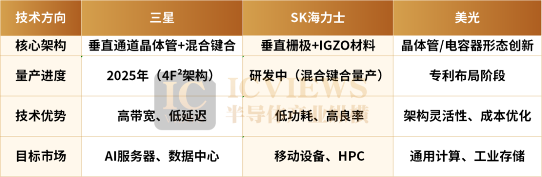
Samsung stands at the forefront of vertical stacking technology. Leveraging Vertical Channel Transistor (VCT) technology, the company stacks transistors vertically, achieving a 30% reduction in cell area. This is further enhanced by the integration of hafnium zirconium oxide (HZO) material, which optimizes charge storage performance. Currently, Samsung has successfully developed a 128Gb 3D X-DRAM sample and aims to introduce commercial products based on the 4F² architecture by 2025. The ultimate goal is to scale up single-chip capacity to 1Tb by 2030.
This technology boasts high bandwidth, low latency, and offers over three times the storage capacity per unit area compared to traditional 2D DRAM.
According to recent Korean media reports, Samsung's Semiconductor (DS) division has outlined a clear roadmap for mass-producing VCT DRAM and has officially commenced related efforts. As part of this roadmap, Samsung is currently mass-producing fifth-generation 10nm-class DRAM and plans to transition to sixth-generation products this year. Following the establishment of a timeline for seventh-generation product development next year, Samsung has made the strategic decision to focus on VCT DRAM for its eighth-generation offerings.
In this new wave of technological competition, SK Hynix is not to be outdone, adopting Vertical Gate (VG) technology. Last year, the company showcased a 5-layer stacked 3D DRAM prototype at the "VLSI 2024" conference, boasting a yield rate of 56.1%.
Their research paper highlighted that the experimental 3D DRAM exhibited comparable characteristics to current 2D DRAM, marking Hynix's first public disclosure of specific data and operational features related to its 3D DRAM development. Furthermore, Hynix is exploring the use of IGZO materials in 3D DRAM to tackle bandwidth and latency challenges. IGZO, a metal oxide material comprising indium, gallium, and zinc oxide, exists in both amorphous and crystalline forms.
Micron embarked on 3D DRAM research in 2019 and, as of August 2022, held over 30 patents related to the technology. This figure surpasses that of Samsung and SK Hynix, the two Korean chip giants, by two to three times. At the IEEE IEDM conference in late 2023, Micron unveiled its advancements in 32Gb 3D NVDRAM (Non-Volatile DRAM). However, according to foreign media outlet Blocks & Files, which sourced information from two industry analysts, this groundbreaking memory technology is unlikely to progress to commercial mass production in the near future. Nonetheless, the technical advancements demonstrated are anticipated to influence future memory products.
-
![]()
OFILM Reports Colossal 460 Million Yuan Loss: Founder Quietly Shifts Focus to Optical Modules!
-
![]()
Yutong Optics and Zeiss Forge Partnership to Develop Quality Measurement System and Launch "Optical Communication Joint Measurement Class"
-
![]()
AutoNavi Revises Splash Screen Ads with Precision Amid Controversy
-
![]()
Unlicensed Vehicle Disputes: AutoNavi Ensnared in the Aggregation Model
-
![]()
Agent: The 'Hard Requirement' for Entering Core Enterprise Systems for the First Time
-
![]()
Global Auto Market Outlook: Sales Decline in China, US, and Europe, Chinese Exports Approach 10 Million
-
![]()
AI Pioneer Breaks Free from the 'Doldrums'
-
![]()
Valuation Exceeds $26 Billion! Three Chinese "Gold Medalists" Shake Up the AI Industry