Is NVLink Still NVIDIA's Competitive Advantage?
 06/12 2025
 980
980
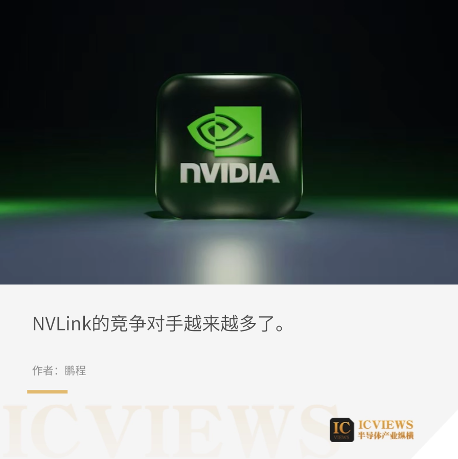
In the realms of AI and high-performance computing (HPC), NVIDIA maintains a dominant position in the industry, underpinned by its diverse core technologies. Among these, in addition to its renowned AI hardware and CUDA ecosystem, the NVLink memory sharing port technology stands out as a key competitive advantage, solidifying NVIDIA's market position. However, as technology evolves and industry competition intensifies, the stability of NVLink's role as a competitive moat has garnered significant attention.
How Does NVLink Fortify NVIDIA's AI Moat?
In 2014, NVIDIA unveiled the NVLink protocol, heralding a new era for multi-GPU collaboration. In 2016, NVLink 1.0 made its debut in the DGX-1 system, seamlessly connecting 8 P100 GPUs. At the time, traditional PCIe (Peripheral Component Interconnect Express) interconnection technology was constrained by bandwidth and latency, struggling to meet the escalating demands of HPC applications. NVLink 1.0 emerged with a bandwidth of 80GB/s, effectively alleviating data transmission bottlenecks, substantially enhancing multi-GPU system collaboration efficiency, and reshaping the landscape of HPC multi-GPU collaboration.
Since then, NVLink has undergone several significant technological advancements, continuously pushing performance boundaries. In 2017, the introduction of NVLink 2.0 introduced the pivotal NVSwitch component, further scaling the connection capacity. With NVSwitch, multi-GPU and CPU nodes can construct intricate interconnect networks on a grander scale, with each link's bandwidth increased to 25GB/s and bidirectional total bandwidth reaching 50GB/s. For instance, the V100 GPU supports up to 6 links, achieving a bidirectional total bandwidth of 300GB/s, providing robust support for large-scale computing tasks.
The 2020 release of NVLink 3.0 marked another technological leap, doubling the data transmission rate of each differential pair to 50Gbit/s while optimizing the number of differential pairs from 8 to 4. The Ampere architecture-based A100 GPU, with its 12 links, offers a total bandwidth of up to 600GB/s, significantly boosting data transmission efficiency.
By 2022, NVLink 4.0 introduced a pivotal signal technology innovation, transitioning from NRZ to PAM4. GPUs based on the Hopper architecture achieved a total bandwidth of 900GB/s with 18 NVLink 4.0 links, further cementing NVIDIA's technological supremacy in high-speed interconnection. At COMPUTEX 2025, NVIDIA's fifth-generation NVLink escalated bandwidth to an astonishing 1.2TB/s, continually setting new performance benchmarks in HPC.
Moreover, as technology advances, NVLink's application scenarios have continuously expanded. In AI and deep learning, AI model training, especially for large language models, necessitates processing colossal parameters and data, far exceeding the memory and computing power of a single GPU. NVLink enables multiple GPUs to share a unified memory pool, accelerating model training.
As technology continues to advance, NVLink's application scenarios continue to broaden. In AI and deep learning, training large language models poses immense challenges in handling massive parameters and data, surpassing the capabilities of a single GPU. NVLink technology facilitates multiple GPUs to share a unified memory pool, dramatically accelerating model training through efficient data transmission and collaborative computing. Real-world test data indicates that an NVLink-interconnected thousand-card cluster achieves over double the parameter synchronization efficiency, with overall computing power utilization soaring from 60% to 90%. It is precisely through establishing a robust technological barrier with NVLink that NVIDIA has dominated the global AI training market, monopolized the global high-end GPU market, and emerged as a leader in HPC.
NVLink Faces Growing Competition
Currently, NVIDIA GPUs are pervasively used in various high-compute fields globally due to their efficient computing capabilities, making NVLink the de facto industry interconnection standard. However, this situation has also sparked competition from other tech giants. To compete with NVIDIA in HPC and AI, AMD and Intel have introduced interconnection solutions like CXL and UCIe. These competitors confront a dilemma: if they fail to accelerate compatibility and adaptation to market demands and existing ecosystems, their products may be marginalized in fierce competition; alternatively, they must invest heavily in technology research and development and market promotion.
Furthermore, intra-industry competition is intensifying. The UALink Alliance recently released the 1.0 standard, introducing new technological options to the market. Beijing Tanwei Xinlian Technology Co., Ltd., the first domestic provider of interconnection communication solutions comparable to NVIDIA's "NVLink & NVSwitch," also announced the completion of tens of millions of RMB in angel round funding. Originating from Tsinghua University's Brain-Inspired Computing Research Center, Tanwei Xinlian focuses on GPU-to-GPU communication protocol and switching chip research and development. Its self-developed ACCLink & ACCSwitch technology rivals NVIDIA's NVLink & NVSwitch in performance and functionality, infusing new vitality into domestic HPC interconnection technology development and posing new competitive pressures on NVIDIA's NVLink technology.
NVIDIA Opens Up NVLink
At COMPUTEX Taipei 2025, NVIDIA CEO Jen-Hsun Huang announced the licensing of NVLink Fusion technology, granting access to its high-speed interconnection system to 12 third-party companies, including MediaTek, Marvell, Fujitsu, and Qualcomm. This move is expected to reduce AI server manufacturing costs by 18%. On the surface, opening up NVLink appears to signal NVIDIA abandoning its long-held hardware closed-loop advantage. However, a deeper analysis reveals this as a strategic transformation. By inviting third-party hardware access through NVLink Fusion, NVIDIA aims to expand the CUDA ecosystem's "sphere of influence," transitioning from a pure hardware vendor to a "technological standard output + regional capacity binding" model, shifting its role from "shovel seller" to "road builder."
Recently, NVIDIA debuted NVLink Fusion, officially entering the ASIC market and directly competing with the UALink Alliance. NVIDIA CEO Jen-Hsun Huang stated that 90% of ASIC projects will fail and emphasized that NVIDIA's ASIC products will outpace competitors. However, NVIDIA's decision to license NVLink Fusion technology underscores its concern about its technological moat being breached. With increasing competitors and rapid technological advancements, NVIDIA must consolidate its market position by opening up technology, reflecting growing competition and challenges to its core technology.
Huawei's SuperPod Technology May Disrupt NVIDIA's NVLink Monopoly
Despite NVIDIA opening up NVLink technology licensing, none of the initial 12 licensees are from mainland China. In China, developing related technologies is crucial for building large-scale domestic GPU clusters. Recently, the concept of "SuperPod" has rapidly gained traction in AI circles. Originally proposed by NVIDIA, "SuperPod" addresses the growing parameter scale of large models, necessitating larger GPU clusters, scaling from thousands to tens of thousands, or even hundreds of thousands of cards, with potential for even greater scales in the future. There are two primary methods for constructing large-scale GPU clusters: Scale Up and Scale Out. Scale Up, or vertical scaling, enhances computing power by increasing resources per node; Scale Out, or horizontal scaling, expands scale by increasing node count. For instance, adding multiple GPUs to each server is Scale Up, with each server considered a node; connecting multiple computers (nodes) via a network is Scale Out.
Recently, Huawei announced its groundbreaking AI technology—CloudMatrix 384 SuperPod. This SuperPod, comprising 384 Ascend compute cards, is the largest single unit among currently commercially available SuperPods, offering up to 300 PFLOPs of dense BF16 computing power, nearly double that of NVIDIA's GB200 NVL72 system. Huawei's CloudMatrix 384 SuperPod achieves a significant evolution from "traditional Ethernet" to "shared bus network" through its ultra-high-bandwidth Scale-Up new high-speed bus network, increasing resource interconnection bandwidth by over 10 times and surpassing NVIDIA's NVL72 SuperPod in key features.
This cluster computing technology effectively compensates for domestic chips' deficiencies in advanced processes and computing power. In an interview, Huawei CEO Ren Zhengfei stated, "Single chips still lag behind the US by a generation. We use mathematics to compensate for physics, non-Moore's Law to compensate for Moore's Law, and cluster computing to compensate for single chips, achieving practical results." Ren Zhengfei added, "China has opportunities in mid-to-low-end chips, with dozens or hundreds of chip companies diligently working. In particular, there are greater opportunities in compound semiconductors. For silicon-based chips, we use mathematics to compensate for physics, non-Moore's Law to compensate for Moore's Law, and the principle of cluster computing to meet our current needs." He also said, "There's no need to worry about the chip issue. With methods like stacking and clustering, the computational results are comparable to the most advanced levels. In terms of software, there will be hundreds of open-source software to meet society's needs."
It's worth noting that NVIDIA had SuperPods earlier but could only accommodate up to 72 cards. This is due to NVIDIA's cards communicating via copper cables (NVLink), ensuring hundreds of gigabits per second communication efficiency without CPU involvement. This enhances throughput and efficiency as card count increases for multi-card training and inference. However, NVLink has limitations, as it cannot exceed 3 meters without signal attenuation. Thus, NVIDIA's multi-card SuperPods are confined to a single cabinet, with a maximum of 72 cards.
In contrast, while Huawei's Ascend single-card performance trails NVIDIA, Huawei, with its communications background, holds unique advantages in communication technology. Huawei adopted optical communication instead of copper cable communication. This innovation guarantees higher bandwidth than NVLink over nearly unlimited transmission distances. Consequently, Huawei's SuperPods don't require compute cards to be centralized in one cabinet and can be distributed across different data centers. This advantage allows Huawei to stack compute cards on a larger scale, with the 384 SuperPod's actual compute nodes far surpassing NVIDIA's 72 SuperPod, with further expansion potential. Additionally, Huawei's optical communication technology excels in modularity and heterogeneity, supporting not only Ascend cards but also being compatible with various other TPUs, fostering an open and flexible ecosystem.
NVIDIA Also Aims for Optical Communication Technology
Clearly, NVIDIA recognizes related issues and is investing in optical communication technology and products. NVIDIA prioritizes silicon photonics technology for current and next-generation optical systems. In March 2025, NVIDIA announced the world's first 1.6T CPO system using a new micro-ring modulator and stated that its Quantum-X silicon photonics switch will ship in the second half of 2025, followed by the Spectrum-X system in the second half of 2026.
However, in optical communication technology ecosystem development, NVIDIA faces numerous challenges. Meta and Microsoft advocate building a new ecosystem around CPO and are committed to setting industry standards for optical engine manufacturing, but initial products will be based on proprietary designs. This poses a significant obstacle to large-scale deployment for major customers preferring custom server, switch, and interconnect device designs. To accelerate CPO technology deployment, NVIDIA plans to provide end-users with complete CPO-integrated systems and assume full responsibility for system operation and maintenance. If these systems deliver substantial performance improvements, customers may adopt them. However, in the long term, relying solely on NVIDIA's design is unacceptable for large cloud companies like Meta and Microsoft. To achieve large-scale CPO technology deployment, building a new and competitive ecosystem is crucial.
Broadcom also recently announced the delivery of the Tomahawk 6 switch series chip, offering a per-chip switching capacity of 102.4 Tbps, doubling the current market's Ethernet switch bandwidth. Designed for the next generation of scalable and extensible AI networks, Tomahawk 6 offers greater flexibility by supporting 100G/200G SerDes and co-packaged optics (CPO).
-
![]()
OFILM Reports Colossal 460 Million Yuan Loss: Founder Quietly Shifts Focus to Optical Modules!
-
![]()
Yutong Optics and Zeiss Forge Partnership to Develop Quality Measurement System and Launch "Optical Communication Joint Measurement Class"
-
![]()
AutoNavi Revises Splash Screen Ads with Precision Amid Controversy
-
![]()
Unlicensed Vehicle Disputes: AutoNavi Ensnared in the Aggregation Model
-
![]()
Agent: The 'Hard Requirement' for Entering Core Enterprise Systems for the First Time
-
![]()
Global Auto Market Outlook: Sales Decline in China, US, and Europe, Chinese Exports Approach 10 Million
-
![]()
AI Pioneer Breaks Free from the 'Doldrums'
-
![]()
Valuation Exceeds $26 Billion! Three Chinese "Gold Medalists" Shake Up the AI Industry