Glass Substrate: Intensifying Competition Among Tech Giants
 06/15 2025
 1010
1010
A slender glass plate, less than a millimeter thick, is igniting a subtle yet fierce competition between Intel, Samsung, and TSMC.
In this intense AI chip "packaging race," Samsung is methodically advancing its strategic layout of glass interposers. Recent news indicates that Samsung Electronics plans to officially adopt glass interposers by 2028, replacing the current silicon interposer technology.
It's noteworthy that while glass interposers have emerged as a new direction for industry exploration, Samsung's development path is unique. Unlike the widely adopted approach in the industry of using large-size glass panels measuring 510x515 millimeters, Samsung has opted for a different route, focusing on the development of small-size panels smaller than 100x100 millimeters. This move aims to expedite prototype validation, thereby gaining a competitive edge in the market. Although small-size panels may potentially reduce manufacturing efficiency, industry analysts generally believe that this will help Samsung bring related technologies to market faster.
Why Glass?
For a long time, silicon-based materials have firmly occupied the core position in chip manufacturing due to their excellent electrical conductivity and mature process system. However, with the soaring demand for high-performance computing (HPC), artificial intelligence (AI), and 5G technology, the physical limits of traditional silicon-based materials are gradually becoming apparent—heat dissipation bottlenecks, signal delays, and cost pressures have emerged as key obstacles restricting the improvement of chip performance. Against this backdrop, glass substrate technology, with its unique physical and chemical properties, has emerged as a promising breakthrough direction in the field of semiconductor packaging.
Glass boasts excellent dimensional stability and can support larger areas and finer patterns. Its coefficient of thermal expansion is similar to that of silicon, and it is extremely flat and stable.
Additionally, one of the most alluring properties of glass is its low dielectric constant, which minimizes signal propagation delays and crosstalk between adjacent interconnections, crucial for high-speed electronic devices. It also reduces the capacitance between interconnections, enabling faster signal transmission and improved overall performance. In applications where speed is paramount, such as data centers, telecommunications, and high-performance computing, the use of glass substrates can significantly enhance system efficiency and data throughput.
The low dielectric constant also enables better impedance control, ensuring signal integrity throughout the circuit. This is particularly advantageous in radio frequency (RF) applications where impedance matching is crucial for maximizing power transfer and minimizing signal loss. By providing consistent electrical properties across the entire substrate surface, glass substrates aid in the design and manufacture of high-frequency circuits with enhanced reliability and performance.
Another key advantage of glass substrates is their excellent thermal stability, essential for maintaining device performance under fluctuating temperature conditions. Unlike copper-clad laminates, which may deform or delaminate under thermal stress, glass substrates exhibit minimal dimensional changes over a wide temperature range. In applications where thermal management is critical, such as automotive electronics, aerospace systems, and industrial controls, glass can withstand thermal cycling and maintain dimensional integrity under stress, helping to prevent electrical shorts, opens, or other reliability issues typically associated with temperature-induced mechanical strain.
Who Chose Glass?
The low dielectric constant of glass substrates makes them a potential replacement for traditional organic substrates in advanced packaging (such as Chiplet, 2.5D/3D packaging). Leading companies represented by TSMC and Intel have begun to lay out glass substrate research and development, while material giants such as Corning are further reducing production costs by optimizing glass formulations.
TSMC's glass substrate layout is closely tied to its advanced packaging technology roadmap. TSMC has accelerated its layout in the glass substrate field in recent years, viewing it as a key strategic direction for maintaining its advanced packaging technology advantages. In September 2024, TSMC announced that it would vigorously develop fan-out panel-level packaging (FOPLP) technology, clearly identifying glass substrates as the core material, and plans to produce the first batch of glass substrate-based chips for NVIDIA in 2025. This technology addresses the warpage issues of traditional organic substrates (such as ABF carriers) in high-density packaging through the high flatness and low coefficient of thermal expansion (CTE) of glass substrates, while supporting higher interconnection density and signal transmission efficiency.
In terms of the technical path, TSMC focuses on the research and development of Glass Core Fan-Out and TGV (Through Glass Via) processes. According to the planning of Taiwan's glass substrate supply chain, the relevant technical roadmap has been clarified: the Chip-First method will be adopted in 2025, transitioning to the more advanced RDL-First process in 2026, with plans to mass-produce complex TGV processes in 2027, highly synchronized with TSMC's requirements. Additionally, TSMC further enhances packaging performance by optimizing the aspect ratio design of glass substrates (such as achieving an aspect ratio of 20:1 by 2027).
Intel's strategy leans more towards long-term technology reserves and vertical integration of the industrial chain. Its layout in the glass substrate field began about a decade ago, and through continuous R&D investment, it has achieved multiple key technological breakthroughs. In September 2023, Intel announced the industry's first glass substrate technology for next-generation advanced packaging, which significantly improves dimensional stability, via density, and signal transmission speed by replacing the woven glass core in traditional laminates with a solid glass core. According to Intel, this innovation enables a 50% increase in the number of dies placed on the chip, thereby enhancing the density and performance of multi-chip system-in-package (SiP).
To support this technology roadmap, Intel has invested about $1 billion over the past decade to establish a dedicated glass substrate R&D line and supply chain in Arizona, USA, and plans to launch a complete glass substrate solution between 2026 and 2030. The core advantage of this technology lies in its excellent coefficient of thermal expansion (CTE) matching and flatness, which can reduce pattern deformation by 50% while supporting stable processing at higher temperatures, providing guarantees for lithography depth of focus optimization and interlayer interconnection coverage.
Currently, Intel is combining glass substrate technology with co-packaged optics (CPO), targeting the AI chip and high-performance computing (HPC) fields, with related products expected to enter the production stage by the end of 2024. This strategy is seen as an important measure for Intel to continue Moore's Law and consolidate its discourse power in advanced packaging technology, while also driving the entire semiconductor industry's exploration of glass substrates as a replacement for traditional organic substrates (such as ABF carriers). It lays the foundation for future competition in AI chips and heterogeneous computing.
Samsung: Big Achievements with Small Investments
While the industry is beginning to explore glass substrates for interposers, Samsung has adopted a unique strategy. Instead of using large-size glass panels measuring 510x515 millimeters, the company has developed smaller units of less than 100x100 millimeters to accelerate prototype design. The report emphasizes that although the reduction in size may affect manufacturing efficiency, it is expected to speed up the time to market for products.
Samsung's layout in the glass substrate field exhibits a multi-dimensional advancement trend, with its technical roadmap and commercialization timeline gradually becoming clear. Recently, Samsung's Device Solutions (DS) division aims to develop the next-generation glass substrate packaging material – "Glass Interposer," which is intended to replace costly traditional organic plastic packaging substrates and enhance performance, with plans to achieve mass production by 2027. This project has already collaborated with the US material giant Corning, and some production steps may be outsourced to accelerate technology implementation. At the same time, Samsung is jointly working with multiple small and medium-sized enterprises (SMEs) in the materials, components, and equipment fields to tackle the commercialization of semiconductor glass substrates, further strengthening its ecosystem integration capabilities in the field of advanced packaging.
From a timeline perspective, Samsung's glass substrate strategy is divided into two phases: short-term focus on advanced packaging applications and long-term targeting of semiconductor manufacturing. Notably, the glass-based MicroLED large screen released by Samsung at CES 2025 has already demonstrated the potential of glass substrates in packaging size optimization and cost control – large-size rectangular glass carriers can accommodate more chips, thereby improving the production efficiency of advanced packaging.
Furthermore, Samsung is engaged in fierce competition with local Korean rivals LG and SK, as all three parties seek to seize the initiative in the field of chip manufacturing glass substrates. This technology is seen as the next-generation solution to significantly boost chip performance, and with its deep accumulation in the semiconductor business, Samsung is expected to form differentiated advantages in material research and development, process adaptation, and industrial chain coordination.
Currently, Samsung is preparing to use glass interposer packaging for semiconductors in its Cheonan campus, with components provided by external suppliers. The company plans to achieve this goal by leveraging its existing panel-level packaging (PLP) production line. PLP is considered particularly suitable for glass substrates, offering higher productivity compared to traditional wafer-level packaging (WLP) which relies on circular wafers. etnews points out that PLP is expected to improve efficiency by using square panels.
Commercialization Tipping Point
Despite the rapid growth in market demand for glass substrates, their commercialization process still faces multiple technical bottlenecks.
One major obstacle to their application is the lack of uniform standards for the size, thickness, and properties of glass substrates. Unlike silicon wafers, which follow precise global specifications, glass substrates currently lack universally accepted dimensions and characteristics. This lack of standardization poses challenges for equipment manufacturers aiming to produce universally compatible devices, as well as semiconductor factories seeking to replace substrates without making significant adjustments to their processes.
Closely related to standardization is the issue of compatibility, which concerns not only the compatibility between different batches of glass substrates but also the compatibility between the substrate and the semiconductor devices it supports. The unique electrical and thermal properties of glass must be precisely matched with those of the semiconductor devices.
Glass is not typically used in mature products; it will be applied to the most advanced applications and come with better power solutions. However, this presents additional challenges. This is one of its key issues.
As the semiconductor industry moves towards advanced packaging technologies such as chip-scale packaging and 3D-IC, significant changes are occurring in backend processes. This transition involves the adoption and adaptation of methods traditionally associated with frontend semiconductor manufacturing.
As an emerging packaging substrate, TGV technology still presents many difficulties and challenges. TGV technology refers to the key technology of realizing 3D interconnection through processes such as via or blind hole formation, seed layer sputtering, and electroplating filling, using borosilicate glass, quartz glass, etc., as the base material. It is a crucial technology for the application of glass substrates in advanced packaging.
Currently, the development and application of TGV are most mature in Europe, the United States, and Japan. The American glass manufacturer Corning has been dedicated to the research of glass solutions for many years and can provide ultra-large-size glass panels with precision glass containing vias for advanced semiconductor packaging. AGC is a global leading glass supplier that can create vias on thin glass substrates according to customer-specified patterns. LPKF's laser-induced deep etching technology is a new technology widely used in microsystems, capable of processing 5,000 vias per second with a minimum aperture of 5µm. WOP is one of the world's top femtosecond laser micro-machining suppliers, achieving sub-micron precision in femtosecond laser micro-machining. Others, such as Japan's Edion and TECNISCO, are also dedicated to research in the field of TGV, providing solutions for glass substrates.
Today, lithography technology plays a crucial role in achieving line spacings of less than 2µm, essential for packaging using chiplets and 2.5D/3D ICs. However, these finer dimensions also require materials that can withstand more stringent processing conditions while maintaining structural and functional integrity. The biggest challenge currently is how to maximize the utilization of lithography tools.
As packaging imposes fewer restrictions on substrate size and allows the use of larger-size lenses with lower numerical apertures, packaging suppliers are turning to fan-out panel-level packaging (FOPLP) to handle more packages per panel, thereby reducing costs. It is estimated that panel costs can be reduced by 30% to 40% compared to circular 300-millimeter wafer fan-outs.
-
![]()
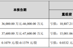
OFILM Reports Colossal 460 Million Yuan Loss: Founder Quietly Shifts Focus to Optical Modules!
-
![]()
Yutong Optics and Zeiss Forge Partnership to Develop Quality Measurement System and Launch "Optical Communication Joint Measurement Class"
-
![]()
AutoNavi Revises Splash Screen Ads with Precision Amid Controversy
-
![]()
Unlicensed Vehicle Disputes: AutoNavi Ensnared in the Aggregation Model
-
![]()
Agent: The 'Hard Requirement' for Entering Core Enterprise Systems for the First Time
-
![]()
Global Auto Market Outlook: Sales Decline in China, US, and Europe, Chinese Exports Approach 10 Million
-
![]()
AI Pioneer Breaks Free from the 'Doldrums'
-
![]()
Valuation Exceeds $26 Billion! Three Chinese "Gold Medalists" Shake Up the AI Industry