Explosion in AI Inference: Can 'Unfortunate' SanDisk Achieve a Phoenix-like Rebirth?
 09/15 2026
 460
460
This round of AI boom has transformed NAND flash memory from a 'cyclically overstocked commodity' into a 'strategically scarce resource in short supply.' After spinning off and shedding the burden of its traditional hard drive business, SanDisk has purely bet on NAND and data center SSDs, precisely hitting this sweet spot.
AI servers require high-frequency, repetitive reading and writing of historical data during inference, processing complex tokens, prompts, multimodal inputs (videos, images), and generating synthetic data. Traditional cloud architecture storage configurations can no longer meet these demands, with AI servers now consuming NAND flash memory at an exponentially increasing rate per node.
During the training-dominated phase, manufacturers focused more on computational power. However, as we enter the inference phase, the formula for AI infrastructure becomes 'AI Infrastructure = XPU + Storage + Connectivity.' While the importance of computational power diminishes, there is a greater emphasis on storage and connectivity needs.
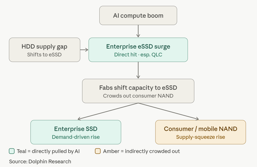
How does AI infrastructure development impact overall industry demand for NAND? In reality, AI data centers do not require all types of NAND products; their primary demand lies in enterprise SSDs. In the current era of Agentic AI and large-scale inference, AI most urgently needs ultra-high-capacity enterprise QLC SSDs and high-bandwidth, low-latency PCIe 5.0/6.0 SSDs.
With major downstream CSPs snapping up enterprise SSDs at premium prices and with long-term orders, storage manufacturers are significantly reallocating their production capacity—originally used for smartphones and PCs—to produce AI enterprise products. This 'supply-side squeeze' indirectly affects the overall supply-demand balance in the NAND sector, driving the overall NAND cycle upward.
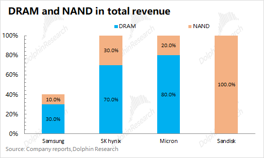
In the NAND market, major players include Samsung, SK Hynix, Micron, and SanDisk, with SanDisk being the most specialized. The top three manufacturers still focus heavily on DRAM and HBM, while SanDisk, after shedding its traditional hard drive business, concentrates entirely on the NAND flash memory market and is poised to fully benefit from the current industry upswing in NAND.
Regarding SanDisk, this article by Dolphin Research primarily addresses three questions: (1) SanDisk's relationship with Western Digital; (2) SanDisk's cooperation with Kioxia; (3) How SanDisk's NAND technology stacks up in the industry. Subsequent discussions on SanDisk's financial performance and valuation will be covered in the next article—stay tuned.
In terms of technological strategy, SanDisk does not 'stubbornly' pursue higher layer counts but instead focuses on 'lateral shrinking' to achieve the industry's highest bit density. It was the first to mass-produce CBA bonding architecture to enhance performance and energy efficiency and jointly introduced HBF (High Bandwidth Flash) technology tailored for AI inference. Overall, SanDisk's technology remains in the relatively leading first tier among NAND manufacturers.
As AI large model inference drives strong demand for ultra-high-capacity enterprise QLC SSDs, SanDisk, with its solid capacity guarantees extended to 2034 through cooperation with Kioxia, high earnings elasticity from being a 'pure-blood NAND' player, and potential opportunities with HBF, will continue to reap growth dividends from AI infrastructure development.
Below is a detailed analysis.
1. SanDisk and Western Digital: A Decade of Itch, Mutual Benefits in 'Separation'
First, let's examine what kind of company SanDisk is. Although SanDisk has not been listed for long, it is a veteran in the storage industry. Founded in 1988, SanDisk is one of the pioneers of flash memory technology and was acquired by Western Digital for approximately $16 billion in 2016.
Due to the distinct growth trajectories and development logics of HDD and NAND products, the combined company faced market 'undervaluation discounts.' In October 2023, Western Digital announced plans to spin off its flash memory business into a new publicly traded company under the SanDisk name, with Western Digital focusing solely on hard drive operations and achieving a 'separate' listing by February 2025.
At the time of the spin-off, Western Digital retained a 19.9% stake in SanDisk, which it had reduced to around 5% by June 2025. Western Digital had borrowed approximately $18 billion for the SanDisk acquisition nearly a decade ago and had been under 'heavy debt pressure' since.
With SanDisk's stock price continuously rising, Western Digital planned to liquidate its 'SanDisk shares' to alleviate debt pressure. A February 2026 announcement stated that Western Digital intended to dispose of all 7.5 million SanDisk shares, potentially reducing debt by over $3 billion.
The disposal of these 7.5 million shares occurred in two steps:
(1) 5.82 million shares were disposed of through 'debt-to-equity conversion and public offering in the secondary market.' The specific process involved 'borrowing bridge financing -> using it to redeem all senior notes -> debt-to-equity conversion -> bank resale.'
(2) The remaining 1.69 million shares were disposed of through a 'share-for-share' exchange. Specifically, 'SanDisk shares were exchanged for Western Digital shares, which were then canceled (4.8 million shares canceled).'
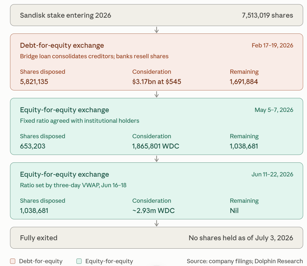
Through these operations, Western Digital's spin-off of SanDisk proved mutually beneficial: (1) Western Digital could focus more on the HDD sector while reducing debt pressure; (2) SanDisk became a fully independent NAND flash memory and SSD company. The two sides are now completely decoupled in terms of equity, with SanDisk having independent control and no longer needing to consider HDD operations.
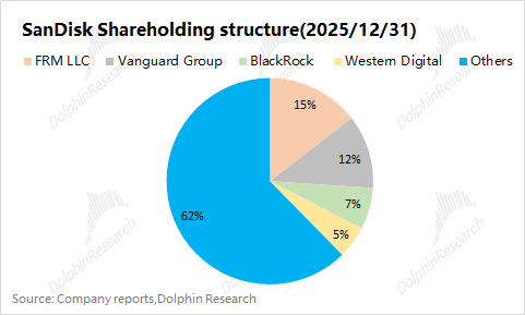
As of the end of 2025, Western Digital remains one of SanDisk's major shareholders. However, after Western Digital fully divests its SanDisk shares, SanDisk will become an independent tech company controlled by Wall Street institutions, with major shareholders including Fidelity Investments, Vanguard Group, and BlackRock. Western Digital's 'selling pressure' has been absorbed.
2. SanDisk + Kioxia: Over 20 Years of Continuous Cooperation
Compared to manufacturers like Micron, SanDisk's product portfolio is more 'singular,' with all revenue derived from the NAND sector. Initially, the AI boom focused on HBM, and SanDisk did not benefit at that time. However, as the storage cycle shifted toward NAND, 'all-in NAND' SanDisk demonstrated greater elasticity.
From an industry perspective, current NAND shipments primarily come from Samsung, SK Hynix, and Micron, with Kioxia and SanDisk following closely, holding roughly 15% of the market share each.
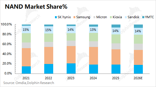
SanDisk and Kioxia have long maintained similar market shares. It is important to note that SanDisk's production capacity primarily comes from Japanese joint venture factories, with wafer capacity evenly split between SanDisk and Kioxia (roughly a 4:6 ratio).
Although Toshiba (Kioxia's predecessor) invented NAND, it lacked the capital and system integration experience for large-scale commercialization, while SanDisk possessed the relevant technology and market channels. Thus, around 2000, the two sides decided to establish a wafer plant in Yokkaichi, Japan:
(1) Joint investment: Purchasing semiconductor manufacturing equipment (lithography machines, etc.) to share heavy asset risks;
(2) Shared R&D: Collaborating in the same laboratory on BiCS architecture development (pre-die stages were jointly researched), with technology shared. Post-die stages were differentiated through proprietary R&D by each company;
(3) Capacity allocation: Wafer capacity was evenly split, with each company taking roughly half (front-end capacity) for independent sales.
SanDisk's cooperation with Kioxia has been exceptionally stable, surviving SanDisk's acquisition and subsequent independence, as well as Toshiba Memory's rebranding to Kioxia, without any interruptions to their cooperation agreements. After becoming independent, SanDisk announced in January 2026 an extension of its original joint venture agreement with Kioxia—set to expire in 2029—to December 31, 2034, ensuring continued cooperation.
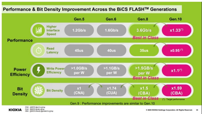
On the same day, both companies announced the sampling of BiCS10 engineering samples in July 2026, with identical specifications—332 layers, 1Tb TLC, density exceeding 29 Gb/mm², a 59% increase over BiCS8, interface speed at 4.8 Gb/s (+33%), and continuing to use CBA and OPS technologies introduced in the 8th generation.
Currently, SanDisk's NAND wafers primarily come from two large-scale bases in Japan: (1) Yokkaichi Base, the world's largest flash memory production site, housing multiple factories including Fab3 to Fab7; (2) Kitakami Base, an emerging incremental site, housing K1 and the newly operational K2 factory.
Kioxia announced on August 27 that it had commenced site preparation and related work for Fab3 at its Kitakami plant, located south of Fab2, targeting production startup in FY2029 to expand advanced BiCS FLASH capacity.
On the same day, both companies announced plans to invest over $31 billion (approximately ¥5 trillion) in Japan by 2032 (within the extended cooperation agreement), contingent on government support. Market estimates suggest K3 will account for roughly ¥1.8 trillion ($11.3 billion) of this investment.
3. NAND Stacking Technology Capabilities and Economics
When NAND products evolved from 2D to 3D, the competition shifted beyond mere process node advancements to layer stacking. Increasing 3D NAND capacity no longer relies solely on process shrinking but can be achieved by adding more layers, breaking free from the 'dead end' of process nodes.
Increasing NAND stack layers directly enhances storage density, meaning NAND supply can be boosted with relatively low capital expenditure. Thus, each manufacturer's layer progress reflects its product capabilities in the NAND sector.
a) Stacking Technology Choices
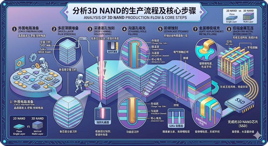
As stack layers continue to increase, the primary technical challenge lies in deep trench etching: specifically, creating billions of holes just tens of nanometers in diameter vertically through 200-300 film layers.
When single-layer etching reaches 200-300 layers, it approaches its physical limits. Imagine precisely piercing hundreds of sheets of paper with a thin needle without breaking or deviating, and maintaining the hole diameter at the bottom.
Above the 200-layer threshold, manufacturers like Micron and Samsung generally adopt a dual-stack approach: 'first depositing 100-120 layers of materials and performing the first deep trench etch; then depositing a second set of 100-120 layers and performing a second etch.'
As they advance toward 300 layers, Samsung and SK Hynix have chosen different paths:
(1) Samsung: Plans to achieve higher layer counts through material improvements while continuing with dual-stacking. Fewer stacking steps theoretically enable higher yields and cost advantages. However, Samsung's V9 QLC (286 layers) faced mass production (mass production) delays due to design issues, slightly lagging in the 300+ layer category.
(2) SK Hynix: Considering the increased risks of continuing with dual-stacking (requiring >150 layers per etch), SK Hynix pioneered a triple-stack approach (e.g., 100+110+111), involving three depositions and three etches, with interconnection of via holes between each segment (precise alignment).
Currently, Samsung V9 persists with 'dual-stacking,' while SK Hynix and SanDisk have shifted to 'triple-stacking.' Samsung's next-generation V10 has also confirmed a transition to 'triple-stacking.'
b) Economics of 3D NAND Layer Stacking
Increasing stack layers from the 200-layer level (232 layers) to the 300-layer level (321 layers) not only adds physical layers but also further shrinks cell dimensions horizontally and optimizes peripheral circuit architectures, boosting bit density per wafer by around 50%.
In other words, if a factory upgrades its existing production line from 200 to 300 layers, its total storage product capacity could theoretically increase by half, even with unchanged wafer input.
Since capacity can be enhanced through layer stacking, NAND manufacturers often choose to upgrade existing production lines, which requires significantly less investment than building new lines. This eliminates the need for new plant construction and infrastructure, involving only equipment replacement and additions related to new nodes (deposition, etching, bonding, etc.). Estimated upgrade costs are roughly one-third of new line construction.
On the other hand, as process steps increase (single-stack -> dual-stack -> triple-stack), the number of chemical vapor deposition (CVD), cleaning, and other processes also rises, directly increasing manufacturing costs per wafer.
Based on market estimates, upgrading from 200 to 300 layers could boost capacity by around 50% while increasing costs by about 30%, reducing storage cost per GB by 10-20%. From an economic standpoint, manufacturers will prioritize layer stacking for capacity expansion.
4. Technological Progress and Comparisons Among NAND Manufacturers
Evaluating NAND product performance involves several dimensions, including layer nodes, bit density (Gb/mm²), architecture (CBA bonding/cell type), interface, and read/write performance.
The technological iteration path of NAND primarily revolves around aspects such as layer stacking, bit density, architectural and process improvements, and unit storage capacity. As for Western Digital's choice, instead of solely focusing on increasing the number of layers, the company initially prioritized lateral scaling, pioneered the introduction of CBA technology, and pursued the development of HBF products. Particularly, it focused on increasing the density of pores on a single layer, thereby achieving 'greater capacity per unit area.'
a) Layer Nodes
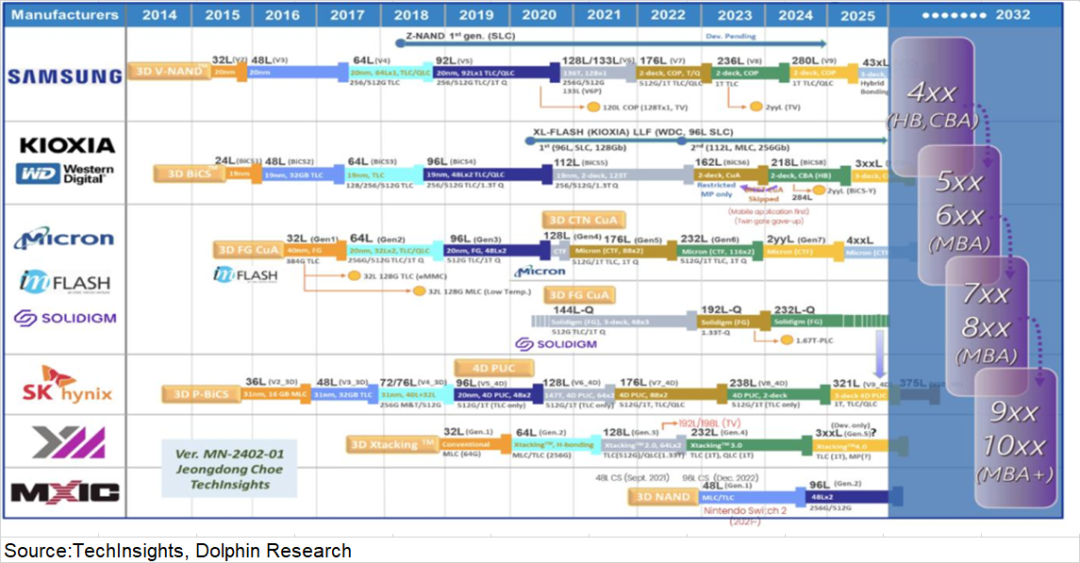
In the NAND market, SK Hynix is currently the leader in layer stacking. The company's 321-layer QLC NAND SSD began mass production and delivery in April 2026, marking it as the world's first QLC product with over 300 layers to enter mass production (utilizing triple-stacking technology).
The progress of the other major players (Samsung, Micron, Kioxia, and Western Digital) in the stacking domain is relatively similar. Based on current mainstream mass production nodes, the ranking is as follows: 321 (SK Hynix) > 286 (Samsung) > 276 (Micron) > 218 (Western Digital/Kioxia).
① Samsung: The V9 QLC (286 layers) experienced delayed mass production due to design flaws but achieved mass production ramp-up after 'rework.' The company repurposed old lines originally running 6-8 generations at Pyeongtaek P1 for V9 production, while also expanding lines at Pyeongtaek P4 PH1 and Xi'an. Currently, V9 accounts for more than half of the production.
Samsung launched the 10th generation BV-NAND (V10) in August 2026, breaking through the 400-layer mark. The company later admitted that it would also adopt the 'triple-stacking' approach for this product.
② Micron: The G9 NAND (276 layers), released in 2024, remains the company's primary shipment product two years later. Micron has shifted its focus to the DRAM sector, resulting in relatively slow progress in NAND. Market expectations suggest that the company's next-generation NAND (possibly G10) will enter mass production only in the second half of 2027.
③ Western Digital & Kioxia: Their current mainstream product is BiCS8 (218 layers). BiCS10 (332 layers) began engineering sampling in July 2026, and the next-generation BiCS11 is already in development.
Due to their shared factory, Western Digital and Kioxia use the same die, such as those based on BiCS8 or BiCS10. However, both companies achieve product differentiation through self-developed controllers and related firmware.
b) Bit Density (Gb/mm²)
Although relatively behind in layer stacking, Western Digital & Kioxia boast the highest areal density. This is because their roadmap focuses on increasing the number of bits per wafer by enhancing 'storage pore' density and tighter cell packaging, rather than simply increasing the number of layers—which directly drives up capital expenditures for factory construction and process complexity.
The BiCS architecture features 'lateral shrinking.' Specifically, it involves 'thinning the layers' and 'densifying the pores,' thereby enabling more storage bits to be packed into the same area (i.e., reducing the shared area). However, this approach also introduces risks such as increased 'charge interference' and compromised 'read/write lifespan and reliability' when layers are thinned.
Based on this, Western Digital & Kioxia's strategy is to 'target BiCS9 for AI PCs and smartphones, while BiCS10 is aimed at AI inference and enterprise-level applications.' BiCS9 represents a minor iteration over BiCS8, with only a slight increase in layer count (218 layers -> 230 layers).
Since the exact areal densities (Gb/mm²) of products from various companies have not been directly disclosed, market expectations suggest the following approximate rankings: Western Digital & Kioxia BiCS10 (>29) > Samsung V9/V10 (28) > Micron G9 (21) > SK Hynix Gen9 (20).
c) Architecture (CBA Bonding/Cell Type)
① CBA: Western Digital & Kioxia are pioneers in the architectural dimension regarding CBA. They were the first to mass-produce the CBA (CMOS Bonded to Array) architecture in BiCS8 (2024)—where logic wafers and storage array wafers are manufactured separately using their respective optimal processes and then bonded together via Cu-Cu hybrid bonding. This achieves higher storage density, faster I/O, and smaller chip sizes.
Samsung and SK Hynix began using CBA bonding in 2026, while Micron has not yet adopted it but is expected to introduce it at the 300-layer+ level in the future.
The CBA approach enables higher efficiency, as the control circuitry (read/write speed) is not affected by high temperatures. Meanwhile, storage cells can be stacked more densely without circuitry occupying space, allowing for further compression of layer height.
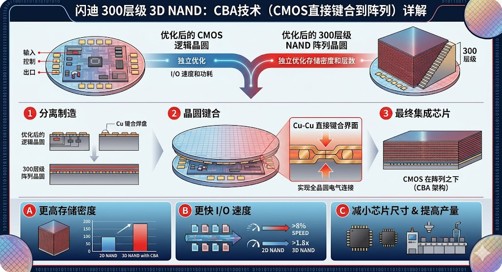
② Cell Type: QLC (4bit/cell) is the mainstream for enterprise-level high-capacity applications—Western Digital's BiCS8 features an 'UltraQLC' 2Tb large die; SK Hynix introduced a 321-layer QLC. Western Digital plans a product structure where TLC (3bit/cell) focuses on performance and QLC on capacity (BiCS9 for 1TB TLC die) and has clarify ly stated it will not adopt PLC (5bit/cell), continuing to rely on CBA + planar shrinking to enhance performance and energy efficiency.
TLC, QLC, and PLC refer to the number of electrons placed in a cell (room). Although the unit storage capacity significantly increases from TLC (3) -> QLC (4) -> PLC (5), the increased number of electrons also affects the lifespan of NAND.
d) Interface and Read/Write Performance (Data Transfer Rate)
Based on the currently disclosed interface rates of three manufacturers, they are relatively close. The data transfer rates of current mainstream products generally range from 3.2-3.6Gbps, while the next generation is expected to increase to 4.8-5.6Gbps.

In reality, the current interface landscape is divided into two camps: Toggle DDR and ONFI. Western Digital & Kioxia and Samsung use Toggle DDR, while Micron and SK Hynix belong to the ONFI camp, with slightly different rate tier settings.
Samsung continues to use the Toggle 5.1 interface in V9, while Western Digital/Kioxia are more aggressive, adopting CBA+Toggle DDR6.0 in BiSC9, primarily targeting high-performance client and enterprise-level SSDs (including AI workloads).
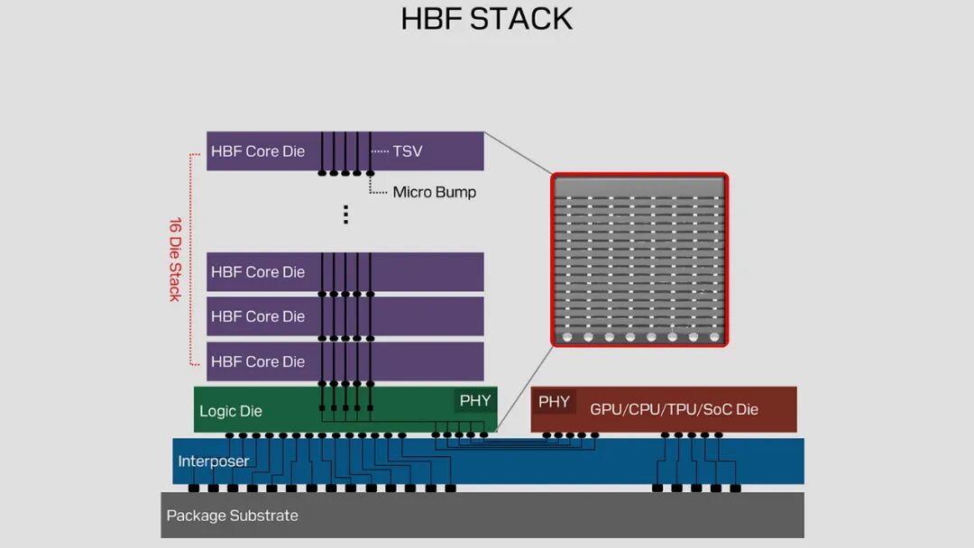
HBF (High-Bandwidth Flash) represents the largest interface variable, with its specifications jointly disclosed by SK Hynix and Western Digital at FMS 2026: It offers two stacking configurations (8-Hi and 16-Hi die) with a maximum capacity of 512GB. The first-generation product aims for approximately 1.6 TB/s bandwidth, microsecond-level latency, and 8-16 times the capacity of HBM, positioning itself between HBM and NVMe SSDs (7-14GB/s).
Traditional NAND is typically connected to the CPU via PCIe after the SSD controller. HBM's speed advantage stems from its 'short distance and wide interface,' directly adjacent to the GPU. HBF applies this package-level interface directly to NAND, enabling it to achieve 'HBM-level read bandwidth + 8-16 times the capacity of HBM.'
It is worth noting that due to differences in physical characteristics, HBF's random read latency is approximately 10us (compared to 10-100ns for HBM), a difference of about 100-1000 times. HBF will not completely replace HBM but rather add a new layer between HBM and SSD, making it more suitable for dense inference scenarios—where weights and large contexts can be prefetched, and slow single reads are acceptable as long as parallelism is sufficient.
Western Digital's HBF progress: The first HBF die has been taped out, with the first batch of inference product samples expected to be delivered in 2027 (CY27).
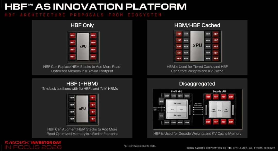
Western Digital outlines four deployment forms for HBF:
① Replacement Type: Pure HBF. Within a similar package area, all HBM stacking positions are replaced with HBF, storing both weights and KV cache in HBF. This maximizes capacity advantage (8-16 times capacity at the same bandwidth) but is the most sensitive to NAND write endurance among the four types (as each token-generated KV directly impacts NAND).
Note: Programming and erasure rely on high voltage to drive electrons through the tunneling oxide layer, leaving trap charges in the oxide layer each time. Once accumulated to a certain extent, the cell can no longer retain charges.
② Cached Type: HBM/HBF Cached. HBM is relegated to the front end as a low-latency cache layer, while weights and KV cache are stored in HBF. This reduces HBF access frequency compared to pure HBF but still imposes write constraints as long as KV data ultimately resides in HBF.
③ Hybrid Type: HBF+HBM Mix. HBF occupies a portion of the stacking positions around the xPU, with the remainder still HBM, dividing labor between the two. This is the lowest-threshold approach—not requiring accelerator vendors to abandon HBM to incorporate HBF, making it the most likely form for first-generation products. Weights are placed in HBF, while KV cache remains in HBM.
④ Disaggregated Type: Disaggregated. HBF is moved away from the compute unit and formed into a separate pool, storing weights and KV cache during the decode stage, accompanied by a smaller HBM layer for caching. Since HBF is unlikely to entirely replace HBM, this approach has the potential to expedite an disaggregated architecture for AI inference—with Google, Meta, SK Hynix, and Tenstorrent in the HBF alliance already pushing in this direction.
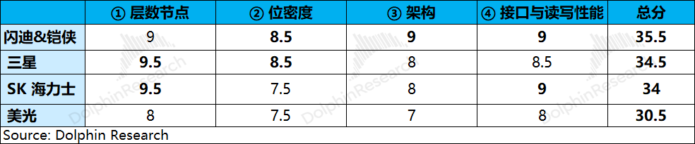
Considering the four main dimensions above, Western Digital's overall technology remains relatively advanced, primarily reflected in bit density, CBA technology, and interfaces (including HBF). Although the company was initially slightly behind in layer count, it has caught up to the leading pack with the mass production of BiCS10.
SK Hynix and Samsung have also begun introducing CBA bonding technology. Meanwhile, Micron remains focused on the DRAM sector, with relatively lower attention to NAND, resulting in slower technological progress in NAND.
In this article, Dolphin Research primarily focuses on Western Digital's relationship with Western Digital Corporation, its collaboration with Kioxia, and the state of NAND technology. The following discussion will center on the company's business progress and valuation pricing. Stay tuned for more.
- END -
// Reprint Authorization
This article is an original work by Dolphin Research. Reproduction is prohibited without authorization.
// Disclaimer and General Disclosure
This report is intended for general comprehensive data purposes, providing users of Dolphin Research and its affiliated institutions with general browsing and data reference. It does not consider the specific investment objectives, investment product preferences, risk tolerance, financial situation, or special needs of any individual receiving this report. Investors must consult with independent professional advisors before making investment decisions based on this report. Any person making investment decisions using or referring to the content or information in this report does so at their own risk. Dolphin Research shall not be liable for any direct or indirect responsibilities or losses that may arise from the use of the data contained in this report. The information and data in this report are based on publicly available sources and are for reference purposes only. Dolphin Research strives to ensure but does not guarantee the reliability, accuracy, and completeness of the information and data.
The information or opinions expressed in this report shall not, under any jurisdiction, be construed as or deemed to be an offer to sell securities or an invitation to buy or sell securities, nor shall they constitute recommendations, inquiries, or endorsements of relevant securities or related financial instruments. The information, tools, and materials in this report are not intended for distribution to or use by individuals or residents of jurisdictions where such distribution, publication, provision, or use would contravene applicable laws or regulations or result in Dolphin Research and/or its subsidiaries or affiliates being subject to registration or licensing requirements in such jurisdictions.
This report merely reflects the personal views, insights, and analytical methods of the relevant contributors and does not represent the stance of Dolphin Research and/or its affiliated institutions.
This report is produced by Dolphin Research, and its copyright is solely owned by Dolphin Research. No institution or individual may, without the prior written consent of Dolphin Research, (i) produce, copy, duplicate, reproduce, forward, or distribute any copies or reproductions in any form whatsoever, and/or (ii) directly or indirectly redistribute or transfer them to other unauthorized persons. Dolphin Research reserves all relevant rights.
-
The 'Three-tier Deconstruction' of the Restructuring Intentions Between FAW and GAC
-
![]()
"Living Room on Wheels": Pie or Trap?
-
![]()
Zhipu Secures Nearly US$5 Billion in Funding
-
![]()
FAW and GAC Integration: Will China's North and South Toyota Further Merge, and Will Dongfeng Continue Its Consolidation Efforts? | MINGJINGpro
-
![]()
Goldman Sachs Sets Its Sights on a City: Ulanqab!
-
![]()
The City in Goldman Sachs’s Spotlight: Ulanqab!
-
How Should Gas Stations Adapt Amid Declining Fuel-Powered Vehicle Sales?
-
![]()
Should GAC Shareholders Be Concerned: FAW Opts Not to Invest Cash but Lightens Its Joint Venture Load to Become Second-Largest Shareholder!