Silicon Carbide Optical Waveguides: From 'Performance Option' to 'Mass Production Element'
 09/28 2026
 340
340
Abstract: By 2026, the role of silicon carbide optical waveguides will undergo a qualitative transformation, no longer serving merely as a performance alternative for AR but evolving into a core element for mass production.
The SiC optical waveguides discussed in this article include both traditional SRG/nano-grating solutions and nano-scale advancements such as metasurfaces/meta-surfaces.
Expansion in materials, chips, and modules is proceeding simultaneously, but cost, processing yield, and supply chain maturity remain three major engineering hurdles that must be overcome before large-scale deployment.
In 2024, Meta Orion's prototype achieved a 70° field of view using silicon carbide optical waveguides, showcasing the potential of SiC materials to the industry.
However, there is a vast gap between 'achieving 70° in the lab' and 'stably delivering 70° on the production line.' By 2026, the situation is changing.
Afalon completed a B-round financing exceeding 100 million yuan to establish an 8-inch SiC meta-surface optical waveguide chip mass production line. Guangna Siwei secured nearly 200 million yuan in financing to enhance full-color SiC optical waveguide production. Goertek Optics launched its first 50° SiC optical waveguide module.
SiC optical waveguides are transitioning from 'can it be made' to 'can it be mass-produced.'
01 Why Are SiC's Physical Advantages Irreplaceable?
The core value of silicon carbide in AR optical waveguides stems from the combined advantages of three physical parameters.
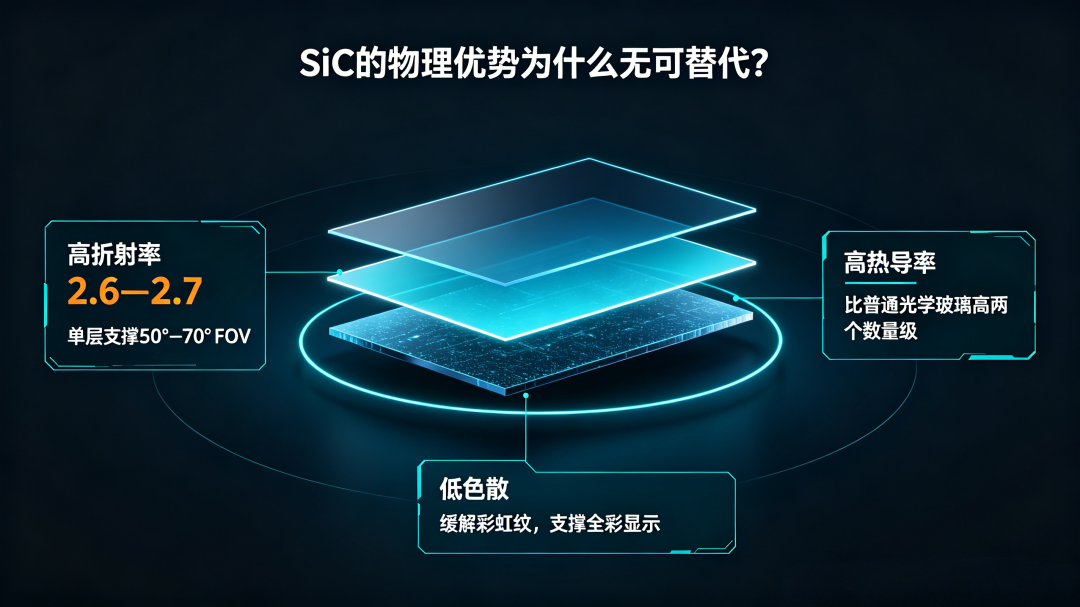
With a refractive index of approximately 2.6-2.7, significantly higher than traditional glass (1.9-2.0) and resin (1.74).
High refractive index enables greater optical étendue and a wider K-domain, allowing a single-layer waveguide to support a 50°-70° field of view, whereas glass solutions typically require multiple layers to achieve around 40°.
Goertek Optics' F50Se module leverages SiC materials to break through the 30° field-of-view physical limitation of glass substrates, achieving 50° FOV.
Thermal conductivity of approximately 490W/mK, two orders of magnitude higher than ordinary optical glass.
This means heat generated by the optical engine can be rapidly dissipated through the waveguide lens itself, eliminating the need for temple-mounted heat dissipation modules and freeing up design space for the entire device.
Low dispersion coefficient below 0.03. High refractive index compresses the effective wavelength of light and reduces grating period, fundamentally mitigating rainbow artifacts in full-color displays.
02 Mass Production Signals in 2026—Three Lines Accelerating Simultaneously
In 2026, the industrialization of SiC optical waveguides is accelerating simultaneously across materials, chips, and modules.
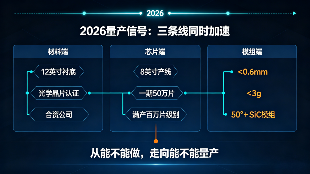
Materials: Tanya Advanced has released a full range of 12-inch SiC substrate solutions, with optical-grade AR substrates extending from power electronics substrate systems to optical waveguide lens processing chains.
San'an Optoelectronics' 6-inch and 8-inch optical wafers have passed certification from international leading clients and are shipping in small batches, with 12-inch wafers having completed sample verification.
Tanke Blue, in a joint venture with Mode Micro-Nano, focuses on technical R&D and market promotion of AR diffractive waveguide lenses.
Chips: Afalon completed a B-round financing exceeding 100 million yuan to establish an 8-inch silicon carbide meta-surface optical waveguide chip mass production line, planning to invest 140 million yuan to build a large-scale manufacturing center for meta-surface optoelectronic chips, with an initial planned capacity of 500,000 wafers, scalable to millions of wafers at full production.
The company claims its single-cell meta-surface and curved photolithography processes offer differentiated advantages, but whether they are 'industry-first' remains to be validated by patents and mass production.
Modules: Guangna Siwei's silicon carbide full-color optical waveguide products are less than 0.6mm thick and weigh under 3g per piece, already in mass application in Coray Air2 commercial AR glasses.
According to publicly available product information, AAC Technologies' high-end SiC substrate solution targets 50°+ FOV, with some sources indicating a color deviation Δu'v' < 0.02 magnitude. Goertek Optics' F50Se module, paired with a full-color LCoS optical engine, achieves over 1500 nits of eye-entry brightness.
03 Why Now?
—Three Industrial Signals The acceleration of SiC optical waveguides is no accident; it results from the simultaneous emergence of three industrial signals.
First, end-user demand is upgrading from 'information prompts' to 'display experience.' Monochrome information prompts are no longer sufficient; consumers demand full-color, large-FOV immersive experiences. AAC Technologies' product roadmap shows that the basic 25° field-of-view version targets AI interaction, while the high-end SiC solution targets 50°-class large-field immersive displays—SiC Coincidentally stuck in full-color FOV At the outbreak point of demand (SiC precisely meets the explosive demand for full-color, large-FOV displays).
Second, manufacturing infrastructure is maturing. According to Goertek Optics, China's first 12-inch wafer DUV lithography and etching mass production line has been built and put into operation. Guangna Siwei has established a fully automated nano-imprint production line with an annual capacity of millions of units. Silicon carbide processing is transitioning from 'laboratory handcrafting' to 'wafer-level mass production.'
Third, capital and industrial chains are forming a positive cycle. Guangna Siwei's current financing round attracted industrial capital such as Guangzhou Industrial Investment, Midea Capital, and the Nano Fund, with existing shareholders continuing to increase their investments. Afalon's financing was co-invested by Deyang State-Owned Assets and Ningbo State-Owned Assets. State-owned capital entering indicates the track is being treated as a strategic direction, but this does not mean mass production risks have disappeared.
04 Ecosystem Collaboration—The 'Friend Circle' of SiC Optical Waveguides Is Expanding
The industrialization of SiC optical waveguides cannot be achieved through a single breakthrough. It requires collaboration across five key areas: substrates, design, processing, modules, and end devices.
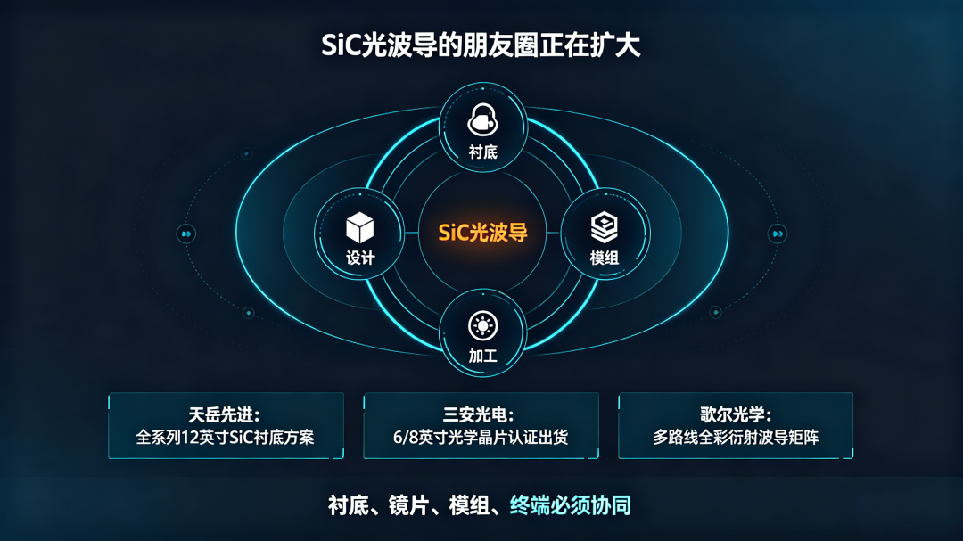
Substrates: Companies like Tanya Advanced, Tanke Blue, San'an Optoelectronics, and Shuo Ke Crystal are accelerating the development of large-size SiC substrates.
Mode Micro-Nano specializes in AR nano-imprint templates and silicon carbide AR diffractive waveguide lenses. Its iterative 50° silicon carbide waveguide achieves over 1000nits/lm luminous efficacy, with combined optical engine display brightness exceeding 3000nits.
At the 2026 OptoElectronics Expo, Goertek Optics showcased a full-color diffractive waveguide product matrix covering multiple technical routes, including glass etching, DUV lithography and etching, nano-imprinting, and large-FOV silicon carbide.
This 'multi-route parallel' product Layout (product Layout should be 'product layout') itself signals that SiC optical waveguides are being integrated into mainstream mass production schemes, rather than remaining mere 'technology demonstrations.'
05 Three Hurdles—Cost, Yield, Supply Chain
The mass production prospects for SiC optical waveguides are clear, but three hurdles must be overcome.
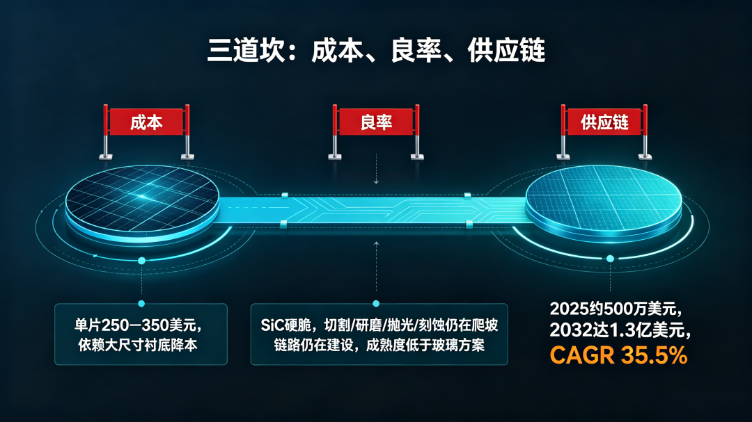
First Hurdle: Cost. In 2025, the global silicon carbide AR optical waveguide market was approximately $5 million (industry report figure: $0.05 billion), projected to reach $130 million by 2032, with a CAGR of 35.5% from 2026–2032. In 2026, it is expected to reach approximately $21 million—a modest scale, but the growth rate indicates industrialization is entering a ramp-up phase.
Currently, the average price per SiC waveguide is $250-350, significantly higher than glass solutions. An 8-inch SiC wafer can yield approximately 4 lenses, while a 12-inch wafer can yield about 10. The number of lenses per wafer remains limited. Scaling effects from large-size substrates are key to cost reduction.
Second Hurdle: Processing Yield. SiC's extreme hardness results in significantly lower cutting, grinding, and polishing yields compared to glass. Silicon carbide etching requires high-precision electron beam lithography and reactive ion etching, with industry yield levels still in the ramp-up phase.
Third Hurdle: Supply Chain Maturity. The complete processing chain for SiC optical waveguides—from substrate → lens rough machining → patterning (electron beam/DUV/nano-imprinting) → etching/imprinting → coating/cutting/bonding → module packaging—is still under construction.
Goertek Optics' 12-inch DUV production line launch is an important step, but for the entire supply chain to reach the maturity of glass solutions, more time is needed. Final Thoughts
Can SiC transition from a 'performance option' to a 'mass production element'? My current assessment is: the direction is correct, but don't expect it to reach consumer-grade pricing before 2027.
Its physical advantages have been validated: higher refractive index enables larger FOV, higher thermal conductivity simplifies heat dissipation design, and lower dispersion fundamentally suppresses rainbow artifacts.
The financing, expansion, and module deployments in 2026 are validating a second point: whether these physical advantages can be stably, economically, and on a large scale ( on a large scale should be 'at scale') replicated.
The answer to the first question is clear. The answer to the second is being written on the production lines.
Interactive Topic: Among the three hurdles of cost, yield, and supply chain for SiC optical waveguides, which do you think is the hardest to overcome? Welcome to leave a comment with your assessment.
—AR Andy | Focusing on optical waveguides and AR microdisplay tracks, deeply dissecting the underlying logic of the optics industry
[Risk Disclaimer] This article is based on publicly disclosed corporate information and industry data, serving solely as industrial commentary and technical popularization of science ( popularization of science should be 'popularization'). Differences in processes and metrics among manufacturers exist, and this does not constitute technical selection or investment advice.]
-
![]()
Changsha Computing Power Firm Lands Another Order Worth Nearly 900 Million Yuan
-
![]()
Jiemei Technology’s Restructuring Plan Greenlit: Set to Acquire Afos Technology for 915 Million RMB
-
![]()
Revenue of 200 Million, Then Another 200 Million Invested! Transight Optoelectronics Takes a Bold Bet on Ultra-Precision Optics Pilot Production
-
![]()
What is the True Value of Zhipu's $3 Billion ARR Amid the 'Data Leak' Controversy?
-
![]()
Monthly Report | China's Online Notebook Computer Market in August 2026: Sales Volume Drops 21%, Apple and Xiaomi Buck the Trend to Gain Market Share; Average Price Rises 12%, Share of Models Priced O
-
【Focus】Low-drag disc brake assembly reduces energy loss and holds great potential in new energy vehicles
-
![]()
Lying Flat in a Car: Is There a 4.4-Fold Increase in the Risk of Severe Injury During a Collision?
-
![]()
Honor Magic9 Pro Max Review: Imaging Gets More Exciting, Agent System Impresses