Are DOE and Metasurfaces Truly Distinct Entities?
 09/29 2026
 499
499

Abstract: There exists a longstanding misconception within the industry that DOE (Diffractive Optical Elements) and metasurfaces are mutually exclusive, iterative alternatives. However, according to Yole's 2025 Diffractive Optics Industry Report, metasurfaces are a nanoscale subclass within the broader DOE family, rather than a replacement. They differ significantly in their physical mechanisms, manufacturing processes, and stages of industrialization. Traditional DOE technology currently supports the mass production of AR waveguides, while metasurfaces pave the way for future enhancements. Clarifying their familial relationship is crucial for understanding the technological evolution in AR optics.
A prevalent confusion in the industry is the perception of DOE and metasurfaces as entirely separate technological paths. Some claim that "metasurfaces will entirely replace traditional DOE," while others simply categorize "DOE as outdated and metasurfaces as the next generation." However, Yole's 2025 report clarifies that metasurfaces are diffractive optical elements with key structural dimensions on the same scale as their operational wavelengths.
To dispel industry myths in one sentence: Metasurfaces are not replacements for DOE but rather a specific subclass within its family. Clarifying this hierarchical relationship is essential for a true understanding of the current state and future evolution of AR optical waveguides.
01 DOE: A 'Technology Family,' Not a Single Device
DOE, or Diffractive Optical Element, serves a straightforward purpose: it modulates light wavefronts using micro-nano structures to alter diffraction propagation directions. Any device that manipulates light waves through diffraction belongs to the DOE technological ecosystem.
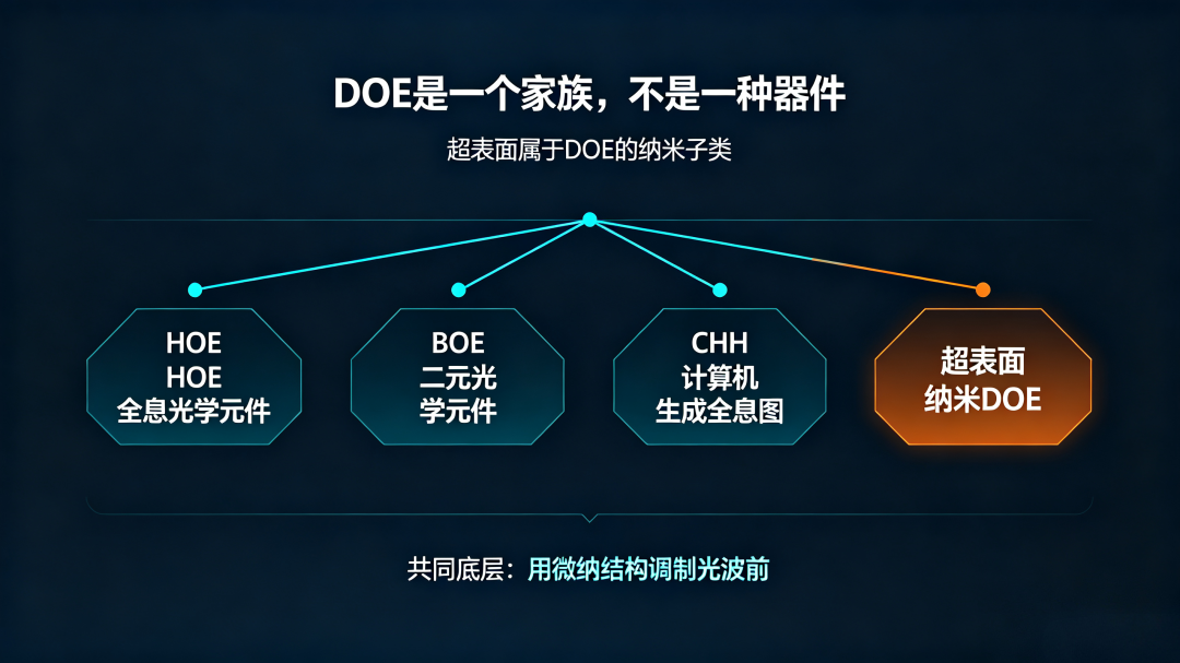
From HOE (Holographic Optical Elements) to BOE (Binary Optical Elements) to CGH (Computer-Generated Holograms), DOE is not a sudden innovation but a family that has evolved through diffraction physics. The earliest holographic optical elements (HOE) originated from Gabor's 1948 holography concept, later iterating into binary optical elements (BOE) and computer-generated holograms (CGH). These devices, with structural pixel sizes larger than their operational wavelengths, are uniformly classified as micro-DOE in the industry.
Since the 21st century, advancements in metamaterials have given rise to metasurfaces, directly compressing DOE structural dimensions to sub-wavelength levels, achieving an upgrade from "micro-DOE" to "nano-DOE." The core function of metasurfaces remains wavefront modulation, identical to the fundamental role of traditional DOE. Their sole distinction lies in the structural scale used for light modulation.
02 Shared Origin, Divergent Principles: Physical Mechanisms Fully Differentiated
Despite belonging to the same DOE family, traditional DOE and metasurfaces fundamentally differ in their phase modulation principles, which is the root cause of their performance limitations and structural variations.
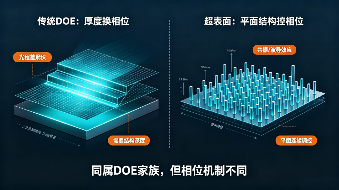
Traditional DOE relies on "optical path difference accumulation." By etching binary or multi-step microstructures on substrates, it creates path length differences across light regions to gradually accumulate the required phase shifts. This physical mechanism imposes inherent limitations: sufficient structural thickness is necessary for adequate phase accumulation, creating a natural ceiling for device thinness.
Metasurfaces employ "planar resonance modulation." Using sub-wavelength nanorods or nanofins as minimal modulation units, they achieve continuous, precise phase control within ultra-thin planes by altering nanostructure dimensions, angles, and refractive indices. Simply put, traditional DOE trades thickness for phase, while metasurfaces control phase through planar structural design. These mechanistic differences lead traditional DOE and metasurfaces toward distinct boundaries in terms of thinness, dispersion, and field of view (FOV)—not as a replacement of the old by the new, but as two branches of the same technological tree.
03 Divergent Manufacturing Pathways: Traditional DOE Uses 'Master Replication,' Metasurfaces Use 'Direct Patterning'
Mechanistic differences further result in entirely distinct mass production logics and process bottlenecks between the two approaches.
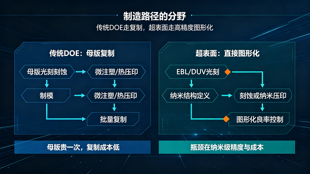
Traditional DOE mass production centers on one-time master fabrication and infinite replication. High-precision photolithography and reactive ion etching create core masters, followed by electroforming or hot embossing to produce molds. Final mass replication occurs via micro-injection molding or hot stamping on polymer or low-melting-point glass substrates. This process's core advantage lies in high upfront master costs but extremely low per-unit replication costs, with high production maturity. Bottlenecks focus on master processing precision and consistency control in large-scale replication.
Metasurface mass production emphasizes high-precision direct patterning, relying on semiconductor micro-nano fabrication systems. Mainstream solutions use electron beam or deep ultraviolet (DUV) lithography to define nanoscale precision structures on silicon, silica, or glass substrates.
Certainly, some AR grating-type metasurfaces have begun adopting nanoimprint lithography for cost reduction, but the fundamental difference remains: metasurface master fabrication still depends on high-precision semiconductor etching processes. Production bottlenecks shift from traditional DOE's "replication consistency" to yield, precision, and cost control in nanoscale patterning, significantly raising production difficulty and entry barriers.
04 AR Optical Waveguide Applications: Traditional DOE for Now, Metasurfaces for the Future
In consumer-grade AR optical waveguide core scenarios, the two DOE approaches have formed clear functional divisions rather than the industry-misreported substitution relationship.
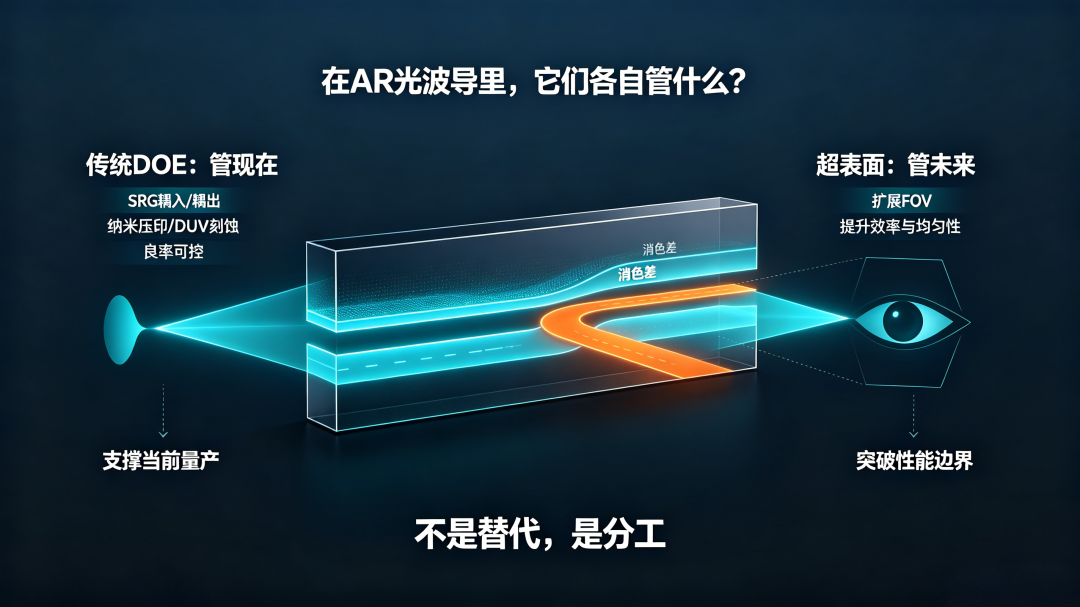
Traditional DOE dominates current AR mass production, exemplified by surface relief gratings (SRG). Leveraging mature nanoimprint and DUV etching processes, SRG gratings reliably handle waveguide coupling functions with strong technological feasibility. Current leading SRG waveguide production yields have risen from early industry lows to over 80%, though industry-wide average yields still hover around 50%, revealing significant tier gaps.
Metasurfaces represent the next-generation upgrade solution to address traditional SRG's inherent shortcomings. Conventional relief gratings suffer from pronounced chromatic dispersion, limited FOV, insufficient coupling efficiency, and poor screen brightness uniformity.
Metasurfaces leverage sub-wavelength structures' precise phase control capabilities to targetedly resolve these pain points: achieving RGB achromatism through multi-diffraction order matching, expanding FOV via high-refractive-index materials + polarization multiplexing, and enhancing coupling efficiency and imaging uniformity through zonal topological optimization.
From an industrial perspective: traditional DOE forms the mass production foundation of AR waveguides, while metasurfaces define their performance ceiling. The two approaches fulfill distinct roles, operating complementarily.
05 Roots of Misconception: Why Does the Industry Insist on Opposing Them?
The frequent industry claim that "metasurfaces will replace DOE" stems primarily from metasurfaces' high visibility as a cutting-edge technology, causing the industry to overlook their essential DOE technological nature.
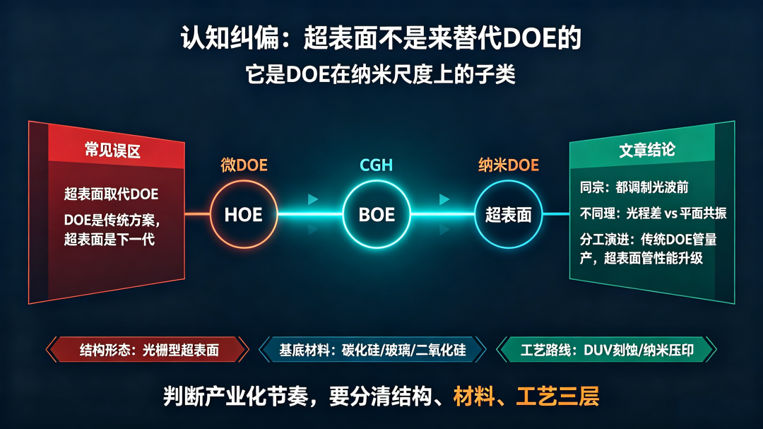
According to Yole's 2025 classification, metasurfaces primarily fall into two forms: grating-type and nanopillar-type. Grating-type metasurfaces mainly serve AR waveguide coupling scenarios; in industry frontiers, some solutions use high-refractive-index substrates like silicon carbide paired with nanoscale gratings to further push traditional SRG's dispersion and FOV ceilings. Nanopillar-type metasurfaces find more applications in 3D sensing and consumer camera modules.
Essentially, grating-type metasurfaces represent nanoscale upgrades to traditional DOE—their core diffraction function remains unchanged, while structural scale and modulation precision achieve leapfrog improvements. Clarifying this relationship is no academic wordplay: determining whether a technology represents a "completely new disruptive path" or an "iteration within an existing system" directly shapes our core judgments about AR optics' industrialization pace, cost reduction cycles, and technological iteration trajectories.
Epilogue
DOE and metasurfaces have never represented a competitive relationship where the new replaces the old but rather a hierarchical family lineage. The evolution from traditional DOE to metasurfaces doesn't involve changing tracks but achieving smaller scales, thinner profiles, and more challenging processes for the same task.
Physical mechanisms upgrade from "optical path difference thickness accumulation" to "planar nanoscale resonance modulation," manufacturing logic iterates from "mold-based mass replication" to "semiconductor-grade high-precision patterning," and industrial stages advance from "mature commercial mass production" to "frontier technology validation and implementation." Understanding this technological genealogy is essential for truly comprehending AR waveguides' core logic in transitioning from viable mass production to ultimate performance.
Discussion Topic: In your work and understanding, do you treat DOE and metasurfaces as separate entities or uniformly manage them within the diffractive optics system? Welcome to share your thoughts.
— AR Andy | Focusing on optical waveguides and AR microdisplay tracks, deeply dissecting the optical industry's foundational logic
【Risk Disclaimer】This article compiles information from Yole's 2025 Diffractive Optics Industry Report and publicly available industry technical data, serving solely as industrial perspective and technical popularization. Technical definitions and process routes vary among manufacturers and do not constitute technical selection or investment advice.
-
![]()
Seres Struggles to Escape Huawei's 'Influence'
-
The AI 'Golden Rice Bowl' of FDE Amid Massive Layoffs
-
![]()
NIO and Geely Cross-Hold Shares: Pioneering a New Auto Industry Joint Venture Focused on Battery Swapping
-
![]()
From 1.3 Trillion to 300 Billion: The Vanishing Trillions in Market Value—Is the Zhipu AI Boom Over?
-
![]()
What Supports Chinese Cinema in the Absence of Blockbusters During the National Day Holiday? | 2026 Chinese Film Report and Overseas Trends
-
US$8.2 Billion: Silicon Valley's Top-Tier 'Girls Help Girls'
-
![]()
Are DOE and Metasurfaces Truly Distinct Entities?
-
![]()
Manus Founder Xiao Hong: Manus Preceded the Advent of Codex and Claude Collaboration