
Tens of Millions in Funding Secured! Can Yuanxi Photonics Surmount the Mass Production Hurdle for Metasurface Optics?
 10/08 2026
 373
373
Recently, Wuhan Yuanxi Photonics Technology Co., Ltd. (hereinafter referred to as "Yuanxi Photonics") successfully closed an angel round of financing amounting to tens of millions of yuan. The investors in this round include CAS Star, Hongshan Capital, Juhuachuanxin, Wuchang Institute, and Jiangcheng Fund. Post-financing, the company is set to concentrate on propelling the research and development of metasurface optical chips and facilitating product rollouts, with a strategic focus on the two significant application markets: intelligent 3D sensing and optical interconnection within data centers.
What enables this optics company, established at the end of 2025, to secure such substantial funding? What is the allure for investors?
Yuanxi Photonics positions itself as a high-performance industrialization platform for metasurface optical technology. Its core team boasts over a decade of expertise in metasurfaces and micro-nano optics, having independently established three technological pillars: full-wave design simulation for metasurface optics, comprehensive full-field and full-parameter automatic optimization, and specialized nano-manufacturing processes.
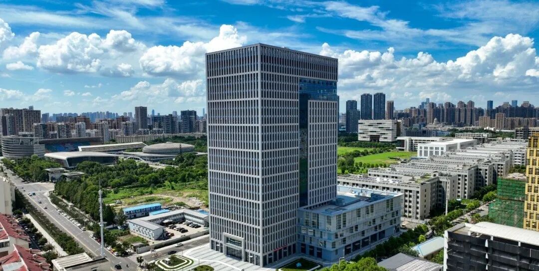
The fundamental principle of metasurface optics lies in harnessing sub-wavelength-scale nanostructure arrays to precisely manipulate the phase, amplitude, and polarization of light. This approach replaces traditional curved lens assemblies with planar, ultra-thin components, thereby enabling the miniaturization and integration of optical systems.
Over the past decade, research in this domain has predominantly remained in the laboratory phase, with manufacturing tolerances, wavelength bandwidth, environmental stability, and wafer-level packaging yields posing as significant barriers between academic breakthroughs and commercial products.
In 2026, a collaborative research team from Sungkyunkwan University and Pohang University of Science and Technology in South Korea pioneered a roll-to-roll nanoimprint technology, achieving a production rate of 300 visible-light metalenses per second at a cost comparable to, or even lower than, traditional refractive optical components. Their findings were published in Nature.
Simultaneously, the demonstration of an 8-inch wafer-level near-infrared all-dielectric metalens signifies that wafer-level mass production pathways are transitioning from conceptual to engineering validation stages. This research, undertaken by teams from the Hangzhou Institute for Advanced Study, University of Chinese Academy of Sciences, and Wuhan University of Technology, employed a step-and-repeat nanoimprint strategy, slashing master mold costs by more than an order of magnitude.
Significant advancements in mass production technology are reshaping capital's valuation logic within the metasurface optics sector, shifting the focus from betting on technological directions to emphasizing process implementation capabilities. Yuanxi Photonics' emphasis on "specialized semiconductor manufacturing process technology" is a direct response to this evolving logic.
The driving force of market demand is also expediting this transformation. According to The Business Research Company, the global market size for "3D sensing technology" is projected to surge from $3.22 billion in 2025 to $3.73 billion in 2026, with a compound annual growth rate of 15.6%. Key drivers include consumer electronics innovation, industrial automation, and the persistent demand for precise depth perception in autonomous driving.
The value of metasurface optical components in 3D sensing scenarios stems from their ability to integrate beam control functions into ultra-thin planar structures, supplanting traditional mechanical scanning or bulky lens assemblies.
Optical interconnection in data centers represents another avenue with explosive potential. According to the Global Metasurface All-Optical Components Industry Outlook Report (2026), the annual demand growth rate for metasurface polarization controllers and mode multiplexers in the communications and data center sectors reaches 67.8%.
The competitive landscape for Yuanxi Photonics is far from forgiving. In the patent arena of metasurface optics, 3M leads with 41 patent families, followed by Lumotive with 25. Avalon Holographics (17), Apple (16), MetaVC (14), Metalenz (13), and others are rapidly expanding their footprint.
Within the domestic industrialization tier of metasurface optics, some companies have already secured tens of millions of dollars in funding for LiDAR and 3D perception directions and have commenced product delivery. Yuanxi Photonics enters the fray with "tens of millions in angel round financing," and its capital efficiency will dictate whether it can accomplish the pivotal leap from process validation to customer adoption within the critical window period.
Metasurface optics stands at the precipice of transitioning from a "technological narrative" to a "production capacity narrative." Capital is no longer solely investing in academic frontiers but is now posing pertinent questions: What is the process yield? What is the unit cost? When will customers be onboarded?
Yuanxi Photonics' angel round financing serves as a signal, but the true litmus test lies not in the financing amount but in whether its metasurface optical chips can achieve their inaugural productized delivery in 3D sensing or optical interconnection scenarios within the next 12 to 18 months. This will mark a watershed moment for metasurface optics to transition from the laboratory to industrialization. The future holds immense promise.
-
![]()
After a model evaluation, I began to re-understand WorkBuddy
-
[Shanhu Talks] The Diverse Lives Unfolding in the AI Era: A Ten-Month Journey
-
【Tibetan Fox Talks】These Ten Months in 2026: People and Me Amidst AI Anxiety
-
Second-Gen Doubao Phone Falls Short in Resolving Previous Flaws
-
Second-Generation Doubao Phone Falls Short in Resolving Previous Limitations
-
![]()
"Dark Side of the Moon" Completes Final Pre-IPO Funding Round with Valuation of Approximately $50 Billion, Kimi Set to List in Hong Kong!
-
![]()
Apple Imposes Mandatory Adaptation Directive for iPhone Duo, Marking Unprecedented Assertiveness
-
![]()
Huawei's Xu Zhijun: The Real Challenge of Super Nodes Transcends Technology