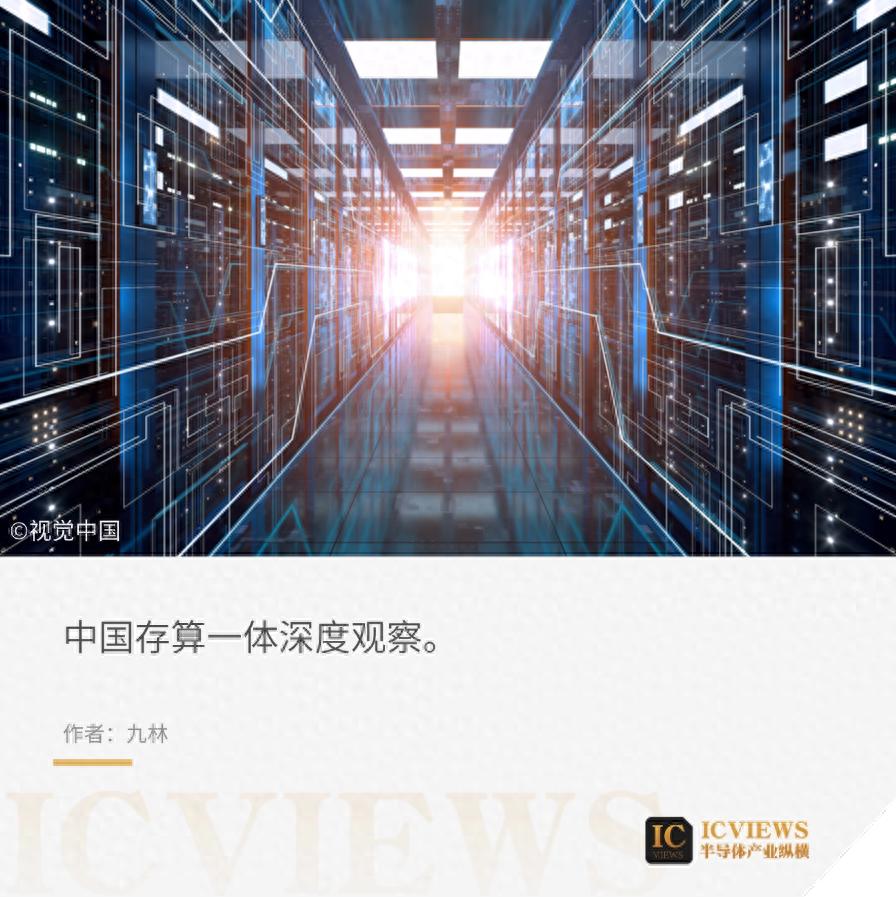
Who is persistently working on Computational Storage?
 04/10 2026
 502
502
In 2026, a long-anticipated technological singularity is approaching.
CCTV’s Xinwen Lianbo (News Simulcast) rarely focused its lens on a cutting-edge chip technology. Feng Dan, a deputy to the National People’s Congress and Vice President of Huazhong University of Science and Technology, called during the Two Sessions for support to establish a world-class Computational Storage industrial base in Hubei, to secure strategic initiative for the country in the new era of “AI Plus.”
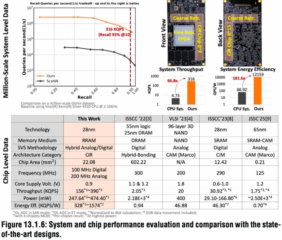
Simultaneously, breakthroughs are occurring at the technical level. At ISSCC 2026, a joint team from Tsinghua University, Huawei, and ByteDance presented a paper on in-memory computing chips, drawing industry attention. The paper introduced, for the first time, a hybrid Compute-in-Memory (CiM) chip based on a 28nm process. Through innovative architectural design, the chip enhances the efficiency and energy efficiency of core operations in recommendation systems by 1–2 orders of magnitude (66x improvement in QPS, 181x improvement in QPS/W).
01
Computational Storage: A Solution in the Post-Moore Era
To understand why Computational Storage is important, we must first grasp a fundamental contradiction: data movement is “eating away” at computing efficiency. Since John von Neumann proposed the stored-program computer architecture in 1945, the global computing industry has developed within this framework for over eight decades. The core feature of this architecture is the separation of computing units from memory units, requiring frequent data transfers between the processor and memory. Imagine a factory where the raw material warehouse is far from the production line: every time a part is made, workers must transport raw materials from the warehouse to the line and finished products back to the warehouse. When parts are small, the drawbacks of this model are not obvious; however, as production scales up, the energy and time consumed by transportation become bottlenecks.
In the chip world, these bottlenecks are vividly named the “memory wall” and “power wall.” Jensen Huang, CEO of NVIDIA, once admitted, “The GPU spends 70% of its time waiting for data.”
As if this were not enough, as semiconductor processes approach physical limits, the performance gains from Moore’s Law are fading, and the cost-effectiveness of traditional chip process scaling is declining, further exacerbating the computing power supply dilemma. The rapid development of large model technologies, exemplified by GPT, has amplified this contradiction. The parameter scale of large language models has grown from billions to hundreds of billions, driving exponential increases in demand for storage capacity and bandwidth.
Against this backdrop, Computational Storage technology has stepped into the spotlight.
The core logic of Computational Storage is straightforward: integrate computing units within memory arrays, enabling data computation directly at storage locations. While seemingly simple, this concept represents a paradigm-shifting innovation in chip architecture.
To put it simply, if traditional chips are like businesses requiring frequent business trips—with computing and memory units in separate locations and data (employees) commuting daily between them—then Computational Storage chips are like businesses that build offices directly inside warehouses: raw materials are at hand, ready for immediate use, resulting in vastly improved efficiency.
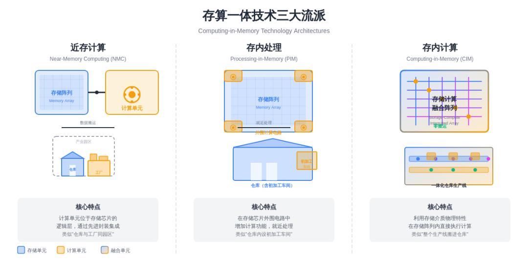
Computational Storage technology has currently evolved into three main schools:
First, Near-Memory Computing (NMC). Computing units are located in the logic layer of memory chips or tightly integrated with memory through advanced packaging technologies. This is akin to building warehouses and factories in the same industrial park—still in separate locations, but much closer. High Bandwidth Memory (HBM) with integrated logic layers or 3D stacking technologies fall into this category.
Second, Processing-in-Memory (PIM). Computing functions are added to the peripheral circuits of memory chips, enabling some computing tasks to be completed directly within the memory. This is like adding preliminary processing workshops inside warehouses, reducing the need to transport all raw materials outside for processing.
Third, Computing-in-Memory (CIM). This is the most integrated approach, directly leveraging the physical properties of storage media (such as resistance, charge, or magnetism) to perform computations within memory arrays. CIM based on SRAM, RRAM (Resistive Random-Access Memory), or MRAM (Magnetoresistive Random-Access Memory) enables highly parallel and ultra-low-power computing. This approach is like moving the entire production line into the warehouse. The chip described in the opening paper belongs to this category.
Each approach has its pros and cons. NMC is the easiest to implement but offers relatively limited improvements; CIM has the greatest potential but poses the toughest technical challenges.
02
A Hundred Schools of Thought: Technical Approaches and Key Players in China’s Computational Storage Landscape
It is predicted that the global market for Computational Storage chips will exceed $12 billion by 2025, with China accounting for 30%. Chinese Computational Storage companies exhibit rich diversity in their technical approaches, driven by exploration of different technical paths and focus on various application scenarios.
In terms of computing paradigms, the main divisions are digital and analog Computational Storage. Digital in-memory computing offers high precision and good compatibility with CMOS processes, making it the mainstream direction for industrialization. Analog in-memory computing achieves higher energy efficiency but is limited in precision. Hybrid digital-analog approaches seek a balance between precision and energy efficiency.
Regarding storage media, the mainstream technical routes include four directions: SRAM, DRAM, Flash, and emerging memristors (ReRAM, MRAM, PCM, etc.), each with distinct technical characteristics and suitable scenarios.
SRAM-based Computational Storage solutions, built on CMOS processes, can utilize advanced process nodes and offer fast read/write speeds but have relatively low storage density and higher static leakage currents. DRAM-based solutions offer higher storage density than SRAM and are suitable for large-capacity model scenarios but have poorer compatibility with CMOS processes. Flash-based solutions provide non-volatility and low power consumption but have relatively slow read/write speeds.
Emerging memristor-based solutions are the most closely watched exploration direction in recent years. New storage media such as ReRAM (Resistive Random-Access Memory), MRAM (Magnetoresistive Random-Access Memory), and PCM (Phase-Change Memory) offer good process scalability and ultra-low power consumption, making them considered the “future” of Computational Storage technology. However, the process maturity and yield of these new media remain the primary bottlenecks restricting industrialization.
It is worth mentioning that advanced packaging technologies are key enablers for high-performance Computational Storage. 2.5D packaging integrates memory and computing units through lateral stacking and interconnection, while 3D packaging achieves vertical stacking and ultimate integration. Currently, TSMC’s proposed 3.5D packaging represents the highest level of packaging in the industry.
Based on different application scenarios, Chinese Computational Storage companies can be broadly divided into two main camps: the “high-computing-power” camp, represented by data centers, intelligent driving, and edge large models, and the “edge AI” camp, represented by smart wearables, smart homes, and IoT. Another underlying thread is foundational technology, with explorers of “new storage media” like XinYuan Semiconductor.
High-Computing-Power and Large Model Directions
These companies primarily target scenarios requiring substantial computing power, such as data centers, high-performance computing, and intelligent driving, aiming to address the “memory wall” and “power wall” challenges in large model training and inference.
Houmo Intelligence is a representative company in the high-computing-power Computational Storage chip field. Its technical approach is based on SRAM Computational Storage and features a self-developed second-generation IPU architecture—Tianxuan. The Tianxuan architecture employs bit-serial computing, integrating computing and memory units for local data processing. Its core technological innovations include Elastic Acceleration technology, which can achieve up to 160% acceleration. Additionally, Houmo Intelligence is the industry’s first Computational Storage chip manufacturer to achieve mass production of floating-point operations, allowing open-source or FP16 floating-point models to run directly without quantized parameter tuning, significantly reducing migration costs for developers. In terms of product progress, Houmo Intelligence released China’s first high-computing-power Computational Storage chip for intelligent driving: Hongtu H30, with 256 TOPS of computing power and 35W power consumption, the first Computational Storage chip for intelligent driving in China. In July 2025, the company announced its second-generation mass-produced chip, Manjie M50, which officially entered mass production in the fourth quarter of 2025.
Yizhu Technology is an AI high-computing-power chip company targeting data centers, cloud computing, and central-side servers based on a Computational Storage architecture. It follows the ReRAM media route and, according to its official website, has independently designed and mass-produced a full-digital Computational Storage architecture high-computing-power chip based on new storage media. Additionally, Yizhu Technology actively embraces the RISC-V ecosystem, being among the first to introduce RISC-V cores in the AI high-computing-power chip field for task scheduling, vector operations, and other functions in large model applications.
Edge, Low-Power, and Edge AI Directions
These companies primarily target scenarios with strict requirements for power consumption, size, and cost, such as smart wearables, smart homes, and IoT devices, achieving efficient edge AI computing through Computational Storage technology.
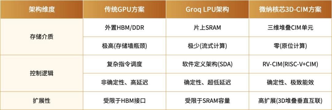
Weina Hexin is a noteworthy company in this space. Its goal is to provide high-performance, low-power, and cost-effective chip solutions for large model inference applications in AI phones, AI PCs, IoT devices, all-in-one machines, servers, and robots. Incubated at the Peking University Information Technology Institute in Zhejiang Province, Weina Hexin follows the CIM technical route. Building on CIM, it integrates “3D Near-Memory Computing” and “RISC-V and Computational Storage Heterogeneous Architecture,” pioneering a three-dimensional Computational Storage (3D-CIM) architecture. Multiple tape-out iterations and testing results show that compared to traditional von Neumann architectures, Weina Hexin’s in-memory computing CIM technology has achieved over 4x improvement in computing density (cost-equivalent improvement) and over 10x reduction in power consumption. In March of this year, GigaDevice invested in Weina Hexin.
Actions Semiconductor is a listed company representative in deploying Computational Storage technology. The company has built a CPU+DSP+NPU tri-core architecture and innovatively adopted SRAM in-memory computing technology, supported by an ANDT toolchain to accelerate algorithm implementation. In terms of technical evolution, Actions Semiconductor is advancing the development of its second-generation in-memory computing IP, aiming to achieve multiple improvements in single-core NPU computing power and energy efficiency optimization while fully supporting the Transformer architecture.
Chipintelli is a representative company in NOR Flash Computational Storage technology. Its core products include the WTM2101 and WTM-8 series. The WTM2101 is the world’s first in-memory computing voice chip based on NOR Flash, officially entering mass production in January 2022. Focused on low-power voice interaction scenarios at the edge, it consumes only 5mW, increasing computing power by 10–200x compared to NPU, DSP, and MCU computing platforms at the same power level. The WTM-8 series is Chipintelli’s new-generation computer vision chip, suitable for low-power, high-computing-power scenarios, supporting the Linux operating system and enabling functions such as AI super-resolution, frame interpolation, HDR, detection, and recognition. This series can provide at least 24 TOPS of computing power while consuming only 5% of the power of similar market solutions.
New Storage Media Directions
XinYuan Semiconductor is a leader in the industrialization of ReRAM (Resistive Random-Access Memory) Computational Storage technology in China, focusing on the research and industrialization of ReRAM new storage technologies. Its core product is a 28nm process ReRAM storage chip, which has entered mass production. The company’s ATOM product series leverages ReRAM’s compatibility with advanced processes to integrate storage and computing units, making it the only company in China to achieve mass production of ReRAM.
ReRAM (Resistive Random-Access Memory) is a new type of non-volatile memory technology offering high storage density, process and CMOS compatibility, and cost-effectiveness. Compared to DRAM, ReRAM significantly increases storage density; compared to Flash, it offers superior read/write performance. XinYuan Semiconductor’s technical route represents an important direction for combining Computational Storage with new storage media. ByteDance’s investment in XinYuan Semiconductor indicates the potential of its RRAM technology in applications such as VR/AR terminal devices.
03
How Is Commercialization Progressing?
Technological leadership is one thing; turning technology into products is another.
Actions Semiconductor’s annual report shows that it has taken the lead in the industry in commercializing in-memory computing technology, officially launching AI audio chips for edge scenarios. The ATS323X chip has quickly landed with flagship wireless microphones from brand clients and is now on the market. It has also entered mass production in wireless gaming earphones from leading domestic brands, and the ATS362X chip has successfully entered the supply chains of multiple leading professional audio brands.
Chipintelli’s WTM2101 chip has shipped over 10 million units, used in smart wearables from brands like Huawei and Xiaomi. This is currently the most successful case of commercializing Computational Storage chips in China, proving the commercial value of Computational Storage technology in low-power edge scenarios. As of now, Chipintelli’s WTM-2 series has been delivered to over 30 customers, with a major order from a leading smart wearable terminal client in the first half of this year.
Houmo Intelligence’s Hongtu H30 chip, released in 2024, is China’s first Computational Storage chip for intelligent driving, having passed AEC-Q100 automotive-grade certification and entering mass production in 2025. The Manjie M50 chip is planned for official mass production in the fourth quarter of 2025 and has established cooperation intentions with leading clients such as Lenovo, iFLYTEK, and China Mobile. Recently, Houmo Intelligence adapted its Kaitian X7 and other information technology-created computers for local lobster processing.
Leveraging its 3D-CIM technology architecture, Weina Hexin has established in-depth cooperation with leading domestic memory manufacturers and multiple terminal industry leaders. It is the only 3D AI chip company deeply cooperating with multiple leading mobile phone companies and coordinating with mobile phone main chip manufacturers. Currently, as the lead unit of the RISC-V Computational Storage Application Group, Weina Hexin has initiated the development of the world’s first RISC-V Computational Storage standard in Xiaoshan, Hangzhou, working with over 20 leading industrial chain companies to promote the construction of an autonomous and controllable AI chip ecosystem.
Yizhu Technology successfully taped out and powered on a high-precision, low-power Computational Storage AI high-computing-power prototype technology verification chip based on new storage media in July 2023, verifying the feasibility of its core technical route. In 2026, it plans to launch a cost-effective and software-compatible domestic AI computing power card.
04
Is In-Memory Computing the Ultimate Solution for Large Models?
As the parameter scale of large models continues to expand, the demand for computing power has reached unprecedented heights. In-memory computing technology, with its unique advantages, holds great promise and is expected to become the ultimate solution to the computing power bottleneck in the era of large models. However, this is not an overnight process but a gradual evolution.
The Evolutionary Path of In-Memory Computing in Ten-Thousand-Card Clusters: Initially, as a dedicated accelerator, it handles specific tasks (such as inference and data preprocessing). At this stage, in-memory computing chips will first serve as a supplement to existing GPU ten-thousand-card clusters, undertaking specific computing tasks.
In the mid-term (here ' mid-term ' means 'medium-term' in English, but kept as a placeholder to show original structure, translate as below in context) medium-term, a hybrid architecture deeply integrated with GPUs will achieve higher-level collaboration. As in-memory computing technology matures and Chiplet (small chip) technology becomes widespread, in-memory computing units will be deeply integrated with general-purpose computing units (such as GPUs or NPUs) through advanced packaging technologies (such as 3D stacking). This hybrid architecture will enable collaboration between 'near-memory' and 'in-memory' computing.
In the long term, new ten-thousand-card clusters dominated by in-memory computing chips may emerge, completely overturning existing architectures. When the process technology and yield of new non-volatile memory media (such as RRAM) reach a high level of maturity, and the versatility and programmability of in-memory computing chips are significantly enhanced, we may witness the emergence of new ten-thousand-card clusters built around in-memory computing chips. Such clusters will completely overturn the existing von Neumann architecture, achieving true 'memory as computing'.
-
![]()
The Surprisingly Significant Impact Difference Between Quiet and Noisy Cars!
-
![]()
Breaking Through Storage Cycle Barriers: How AI Large Models and Coding Technology Synergize to Drive Transformation in the Security Industry
-
Facilitating the Slimming of Camera Modules! O-film Obtains Utility Model Patent for Periscope-Type Reflective Component
-
![]()
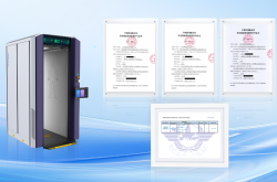
Hikvision Raytine’s Millimeter-Wave Body Imaging Security Inspection Device Achieves ECAC SSc Category A Standard Level 2.1 Certification for European Civil Aviation
-
![]()
Global Market Share for Security Windows Hits 26%! This Optical 'Little Giant' Makes Its Debut on NEEQ
-
![]()
The Evolutionary Path of Agent Engineering: From Prompt to Harness by Zhang Yutao, Co-founder of Moonshot AI
-
![]()
Profits and stock prices are both declining, so why are executives from these auto companies increasing their purchases?
-
![]()
Burning Tens of Billions of Dollars, Yet No Unified Definition for World Models