FPGA+DSP/ARM Architecture Development and Application
 09/29 2025
 634
634
Since the maturation of mid-to-high-end FPGA technology, hardware designs based on the FPGA+DSP/ARM architecture have found widespread application in numerous industrial sectors, such as wireless communications, image processing, industrial control, and instrumentation measurement.
Before the introduction of the ZYNQ series, FPGA+DSP devices were a typical combination used in various industrial applications.
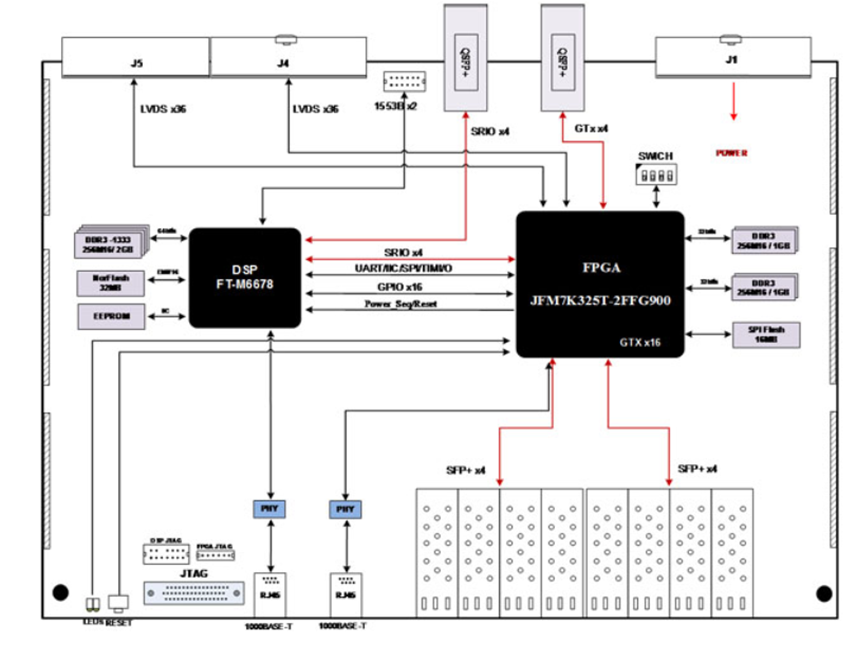
For example, a company utilized a K7325T+6678 combination to launch board cards for wireless communications, radar processing, and image processing. The mid-to-low-end K7325T can handle signal acquisition and processing, while the DSP 6678 connects and transmits data with the FPGA via SRIO for upper-layer processing and applications.
However, from the perspective of flexibility and application scenarios, the inability to implement operating system applications limits the further promotion of the FPGA+DSP architecture.
Additionally, a discrete FPGA+CPU architecture enables hardware logic and software application development, typically allowing interaction and transmission through PCIE and Ethernet interfaces.
As the demands of business scenarios become increasingly diverse, high-level applications such as human-machine interaction and network management maintenance have become indispensable. SOC architectures based on FPGA+ARM/CPU have become the primary application platforms over the past decade.
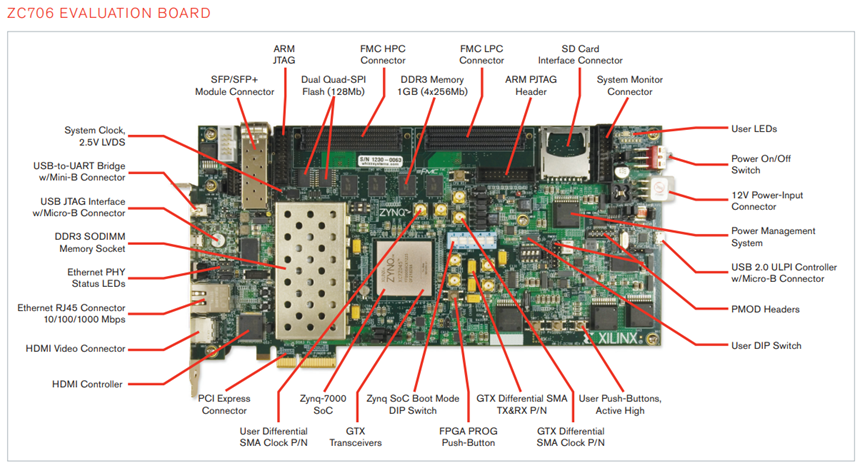
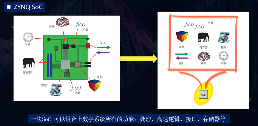
For example, Xilinx's ZYNQ series has become a widely recommended and applied star product in the industry. The PS+PL system and logic development greatly facilitate hardware and software engineers in implementing system functions on a single chip, significantly enhancing system integration and operability.
On a single SoC, system processing, high-speed logic, high and low-speed interface transmission, data storage, and web operation interfaces can all be realized.
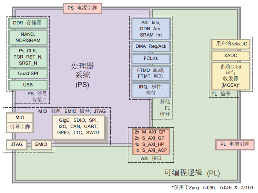
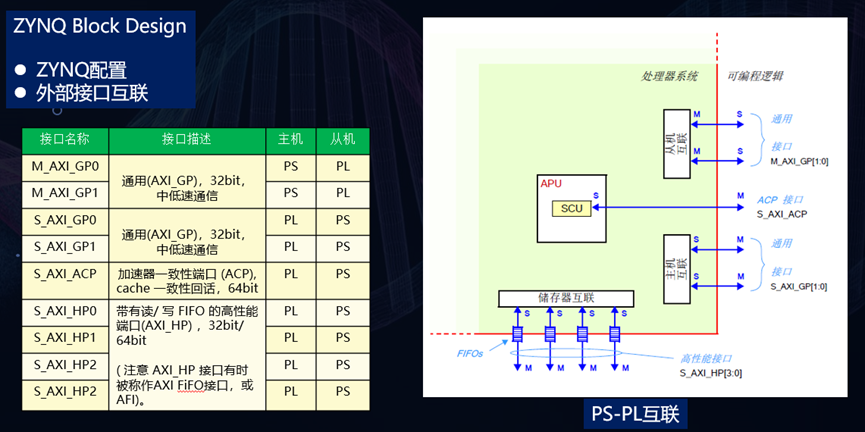
The processor can be seen as the central unit of the hardware system. The ZYNQ part includes rich peripherals and processors, enabling system version loading and control.
The PL side is for pure logic FPGA development. Interaction and transmission between PS and PL can be achieved through interfaces such as GPIO, AXI-Lite, and AXI-Stream.
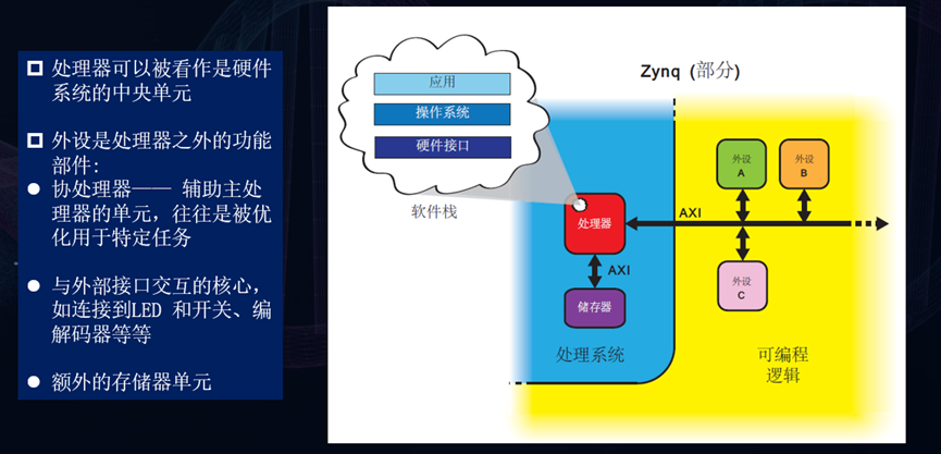
PS and PL are interconnected through rich interfaces. PS can achieve system boot, software processing, and board-level driver support; PL can achieve parallel high-speed processing, interface transmission, storage, temperature monitoring, etc.
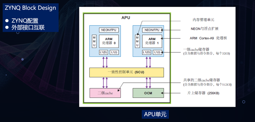
The APU is primarily composed of two ARM processing cores, each associated with several computable units: a NEONTM Media Processing Engine (MPE) and Floating Point Unit (FPU); a Memory Management Unit (MMU); and a Level 1 cache memory (divided into instruction and data sections). The APU also includes a Level 2 cache memory, followed by On-Chip Memory (OCM). Finally, a Snoop Control Unit (SCU) forms a bridge connection between the ARM cores, Level 2 cache, and OCM memory. This unit is also partially responsible for interfacing with the PL, although this interface is not indicated in the diagram.
In product development, a team composed of several members achieves the full process from requirement extraction to customer delivery through division of labor and collaboration.
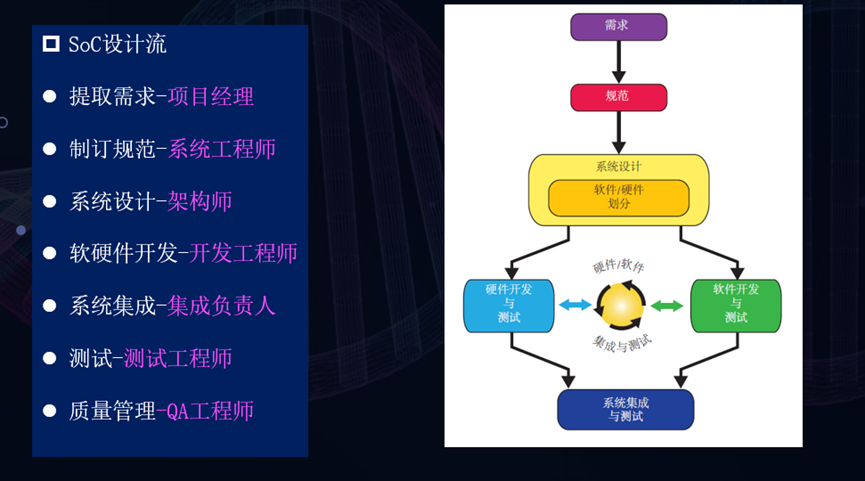
The project manager extracts requirements, decomposes them through project management, and formulates product plans. The system engineer formulates system specifications and oversees critical system design matters. The system architect completes the system architecture design. The designs of software, hardware, and logic architectures are crucial to the product's success. Development engineers are responsible for functional development and verification in their respective fields based on development requirements, including algorithm simulation, self-testing, and data analysis. The integration of each product version involves software and logic bits, with each field integrating and packaging them into a complete version.
Product testing is usually completed by test engineers, while in IC design, it is done by verification engineers. Testing may be divided into unit testing, integration testing, and system testing, depending on the product's complexity.
Additionally, during version output and development processes, quality management sets red lines to ensure product quality through a series of management measures and collaborates with R&D to complete product quality tracking.
In summary, the design flow of ZYNQ is shown in the following diagram, with the PS side responsible for software development and the PL side responsible for logic development, followed by joint debugging.
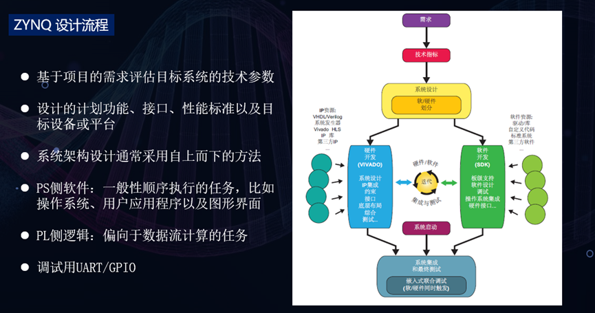
FPGAs are inherently suitable for implementing high-speed parallel computing and thus undertake computationally intensive and highly parallel portions of the system, such as baseband and RF in wireless communications, as well as the data link layer.
The processor on the PS side, equipped with an operating system, enables upper-layer software applications and the running of software protocols.
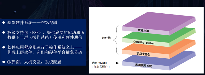
The BSP establishes a transmission channel between software and hardware, enabling hardware-software drivers and data transmission.
The SoC attributes of ZYNQ enable it to meet high-performance computing and application requirements in most scenarios.
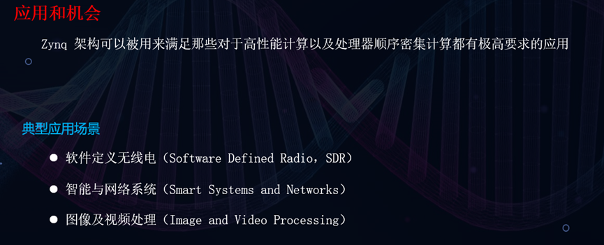
Typical application scenarios include wireless communications and intelligent network systems based on image and video processing.
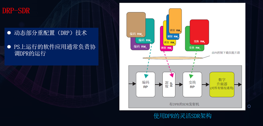
For example, dynamic partial reconfiguration technology can be used to implement software-defined radio systems, enabling rapid waveform replacement.
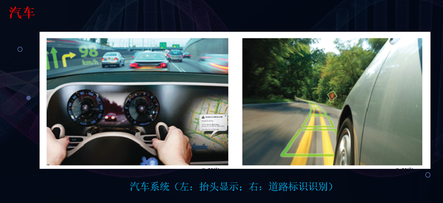
In the automotive sector, it can be used for display control and road recognition.
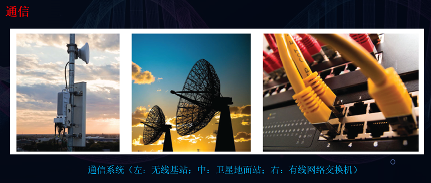
ZYNQ devices are widely used in ground mobile wireless communications, satellite communications, and network switches. FPGAs serve as platforms for computationally intensive processing of packet-switched wireless and wired communications. This field is diverse, including transceivers for ground and satellite transmission, mobile communication backbone networks, wired network equipment, sonar, Global Positioning Systems (GPS), and many other communication systems. For example, low Earth orbit satellite communication systems like Starlink, Oneweb, Guowang, and Qianfan extensively adopt FPGAs for system design.
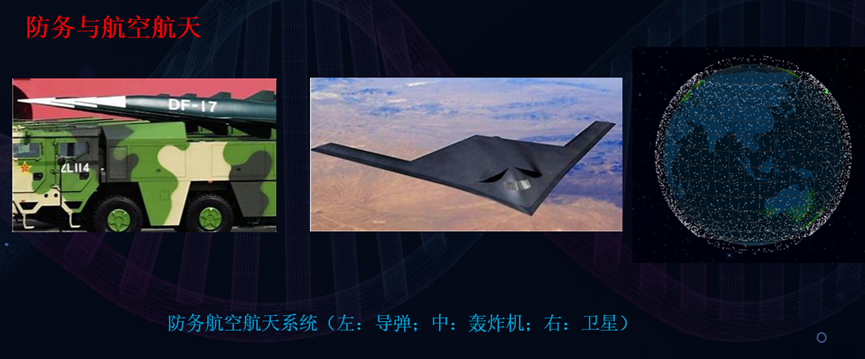
Additionally, in defense security and aerospace fields, FPGA+ARM/CPU/GPU implementations enable data links, satellite-ground communications, or inter-satellite link transmissions. Defense systems encompass various communications, image processing, aviation, navigation, and transportation systems, as well as weapon-related technologies. Military circuits typically require higher robustness, wider temperature ranges, and enhanced security features compared to civilian applications. Civilian aviation applications include navigation and onboard flight systems, satellite and ground communications, and radar systems.
In industrial control, robotics, instrumentation, and other application fields, FPGA+ARM/CPU/GPU play crucial roles. Industrial and scientific processes, ranging from manufacturing and processing to high-energy physics experiments, require precise control and instrumentation. FPGA and Zynq chips are highly suitable platforms because, with the aid of the PL's capabilities, they can rapidly and simultaneously process multiple sensor inputs and operate multiple actuator outputs in real-time. Zynq also offers greater potential for system integration and operational flexibility. For instance, it can monitor the performance of a control loop and switch to software control by reconfiguring it if necessary. If needed, the PS can also support real-time operating systems and/or GUI (Graphical User Interface). Furthermore, ZYNQ is used in instruments such as signal generators, oscilloscopes, spectrum analyzers, vector network analyzers, and channel simulators.
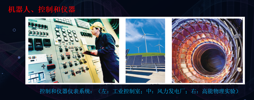
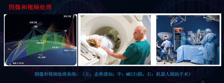
Image and video processing represent another significant application area for ZYNQ, enabling battlefield situation awareness through satellite remote sensing/SAR radar/optical systems, data links, and ad hoc networks. Medical equipment in the medical field (such as CT scanners and endoscopes), robot-assisted surgery, and applications including home and professional cameras, video compression and storage systems, broadcasting equipment, display technologies, industrial process monitoring, security and surveillance, as well as many other uses. Video applications require both deterministic processing of large amounts of pixel data and software algorithms for extracting data from images (which are well-suited for PL and PS, respectively).
Currently, domestic FPGA manufacturers are advancing the design and R&D of domestic ZYNQ SoC devices, with some manufacturers already in the process of tape-out testing and verification. These devices are expected to be launched in the market from the second half of this year to the first half of next year.
High-end devices such as RFSoC and ACAP, serving as upgraded versions of ZYNQ, are used in 5G communications, data centers, and other fields. Domestic equivalents of these device types are relatively lacking and are in a state of catching up or exploring alternative paths.
---
-
![]()
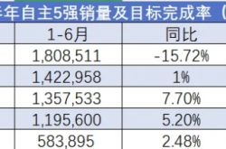
Changan Delivers 1.195 Million Vehicles in H1, Faces Five Key Challenges to Reclaim TOP 3 Spot Over Chery and Geely
-
![]()
Comprehensively Surpassing the "OpenClaw" with the "Hermes": A Lesson for Domestic Agents
-
![]()
In-Depth Analysis: Is Meta Becoming a 'Computing Power Scalper'? Has the Era of AI Infrastructure's Rapid Expansion Come to an End?
-
![]()
Doubao Stealthily Deactivates App Generation Function; No Official Notification Received. Likewise, Qianwen Plans to Deactivate Its AI Agent Function, Possibly Increasing the Barrier for User-Generate
-
![]()
Powerful DJI, Unafraid of Insta360
-
![]()
Why Does the LiDAR Point Cloud Exhibit a “Smearing” Effect?
-
![]()
The Surprisingly Significant Impact Difference Between Quiet and Noisy Cars!
-
![]()
Breaking Through Storage Cycle Barriers: How AI Large Models and Coding Technology Synergize to Drive Transformation in the Security Industry