TSMC North America Technology Symposium: Comprehensive Insights
 05/06 2025
 726
726
On April 23, local time, TSMC held the "2025 North America Technology Symposium" in the United States. The symposium showcased advancements in technology, industry challenges, and opportunities, focusing on AI-driven semiconductor upgrades, advanced process roadmaps, next-generation node verification, and transistor architecture and material innovations, all aimed at supporting future intelligent computing infrastructure.
Here are the key highlights from the symposium:
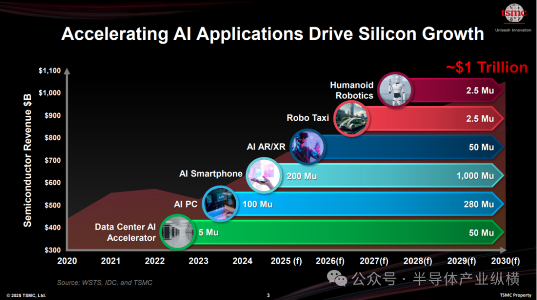
According to the latest TSMC data, the semiconductor industry is entering an unprecedented growth phase. By 2030, the global semiconductor market is projected to reach $1 trillion. The primary driver of this growth is the rapid expansion of high-performance computing (HPC) and artificial intelligence (AI) applications.
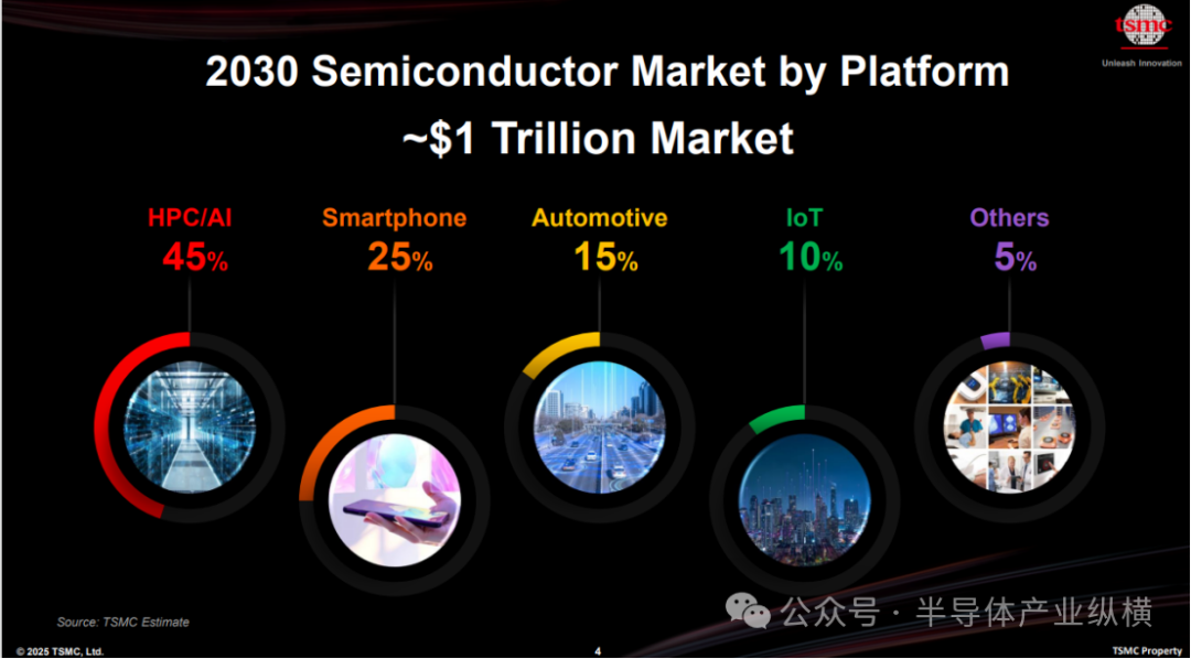
The chart above illustrates TSMC's prediction that by 2030, HPC/AI will account for 45% of the global semiconductor market, becoming the dominant application platform. Following this are smartphones at 25%, automotive electronics at 15%, IoT at 10%, and other sectors at 5%. This shift indicates a transition from a mobile-centric market to an AI and high-throughput computing-driven model.
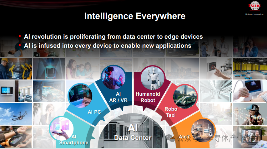
How do AI-driven applications accelerate semiconductor demand? Starting with AI accelerators in data centers, this growth extends to AI personal computers, AI smartphones, augmented reality/virtual reality (AR/XR) devices, and longer-term applications like robot taxis and humanoid robots. These applications are increasing both in number and complexity.
Specifically, shipments of AI personal computers are expected to reach 280 million units by 2029, while AI smartphones could exceed 1 billion units as early as 2025. Additionally, AR/XR device shipments are projected to reach 50 million units by 2028. Next-generation applications like robot taxis and humanoid robots are anticipated to require 2.5 million high-performance chips annually by 2030. These data highlight the need for chips with higher computational performance, energy efficiency, system-level integration, and packaging density.
TSMC believes that these emerging AI-driven applications will significantly increase chip complexity, demand tighter integration, and drive process innovations, ultimately fueling the semiconductor industry's growth towards a $1 trillion market.
N3
Currently, TSMC's N3 series (i.e., 3nm process) includes the mass-produced N3 and N3E, with plans for subsequent versions like N3P, N3X, N3A, and N3C.
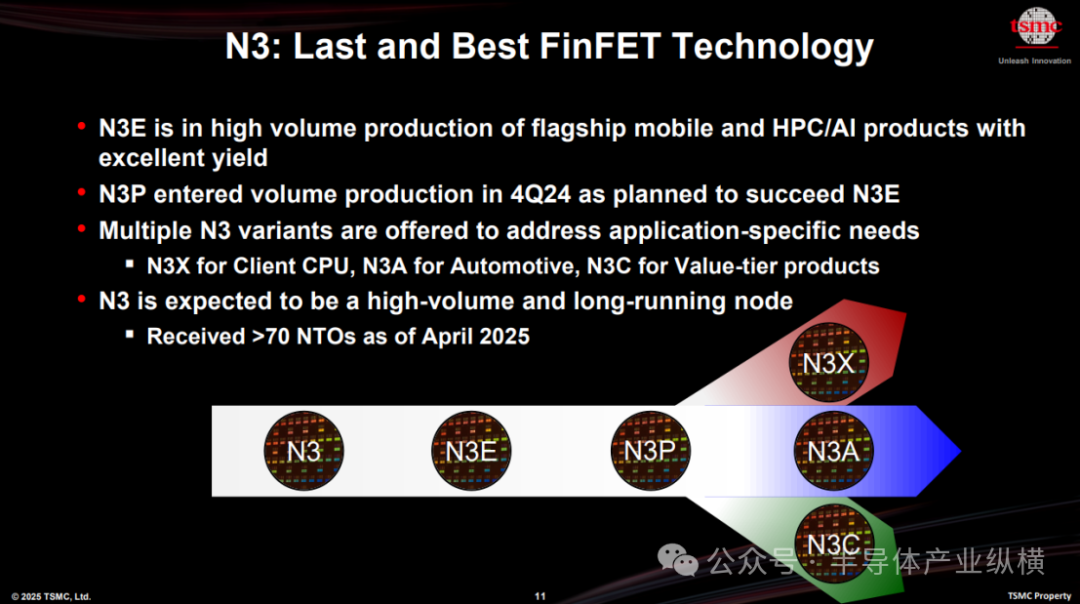
TSMC revealed plans to start production of chips based on the performance-enhanced N3P (third-generation 3nm) process technology in the fourth quarter of 2024. N3P, a follow-up to N3E, targets client and data center applications requiring enhanced performance while retaining 3nm IP. N3P offers a 5% performance boost at the same leakage current or a 5% to 10% reduction in power consumption at the same frequency, with a 4% increase in transistor density for typical mixed designs. Since N3P's density gains stem from improved optics, it benefits high-performance designs that heavily utilize SRAM. TSMC is currently developing products for its major clients based on this technology.
Compared to N3P, N3X is expected to offer a 5% boost in maximum performance at the same power or a 7% reduction in power consumption at the same frequency. However, N3X's primary advantage is its support for voltages up to 1.2V (the limit for 3nm-class technology), providing the absolute maximum frequency (Fmax) for applications like client CPUs. The trade-off for Fmax is leakage power up to 250%, requiring careful design consideration. Mass production of N3X chips is expected in the second half of 2023.
TSMC's roadmap has been extended to 2028, adding N3C and A14. N3C is a compressed version, indicating further process density optimization is possible.
TSMC disclosed the progress of its next-generation chip manufacturing processes at the symposium. The company expects to start mass production of N2 chips in the second half of 2023, marking TSMC's first adoption of fully surrounding gate (GAA) nanosheet transistor technology for production.
N2
N2 (i.e., 2nm process) is TSMC's latest process technology, featuring a nanosheet or surrounding gate design. Compared to N3E, N2 offers a 10%-15% speed boost at the same power consumption or reduces power consumption by 20%-30% at the same speed, with a 15% increase in transistor density. N2 transistor performance is close to the target, with an average yield of over 90% for 256Mb SRAM modules. TSMC expects that driven by smartphones and HPC applications, the number of tape-outs for 2nm technology will exceed those for 3nm and 5nm technologies in the early stages of production.
TSMC continues its technology improvement strategy with N2P, an extension of the N2 series, scheduled for production in 2026. Following N2, TSMC will move on to the A16 (i.e., 1.6nm) node.
A16
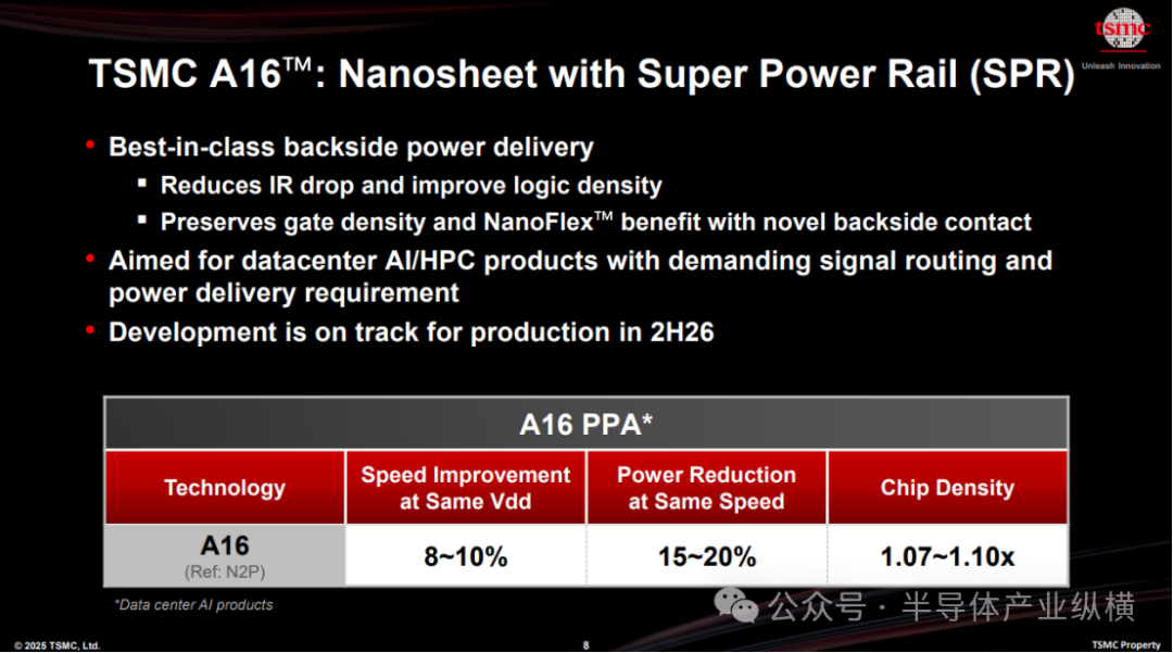
A16's core technical feature is the super power rail architecture, also known as back-side power delivery technology. By moving the power delivery network to the back of the wafer, this technology enhances the chip's logic density and overall performance. Compared to N2P, A16 offers an 8%-10% performance boost at the same voltage and design conditions, with a 15%-20% reduction in power consumption at the same frequency and transistor count, and a density increase ranging from 1.07 to 1.10 times. A16 is particularly suitable for HPC products with complex signal routing and dense power delivery networks, with mass production planned for the second half of 2026.
A14
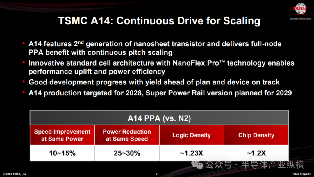
The introduction of the new A14 process technology was a highlight of the symposium. Based on TSMC's industry-leading N2 (2nm) process, A14 leverages second-generation GAA transistor technology (NanoFLEX transistor architecture) to provide faster computation and better energy efficiency, driving AI transformation and potentially enhancing edge AI capabilities for applications like smartphones. A14 is expected to enter mass production in 2028, with progress so far smooth and yield performance better than expected.
In advanced packaging, TSMC also announced several important developments.
TSMC has launched the 3DFabric platform, a comprehensive suite of 2.5D and 3D integration technologies, including CoWoS (Chip-on-Wafer-on-Substrate), InFO (Integrated Fan-Out), and SoIC (System on Integrated Chips). These platforms aim to overcome the scaling limitations of traditional monolithic designs, supporting chiplet-based architectures, high-bandwidth memory integration, and heterogeneous system optimization.
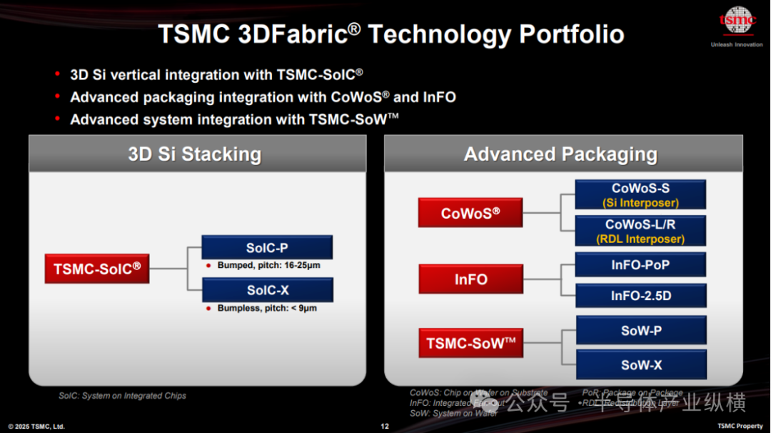
For 2.5D/3D integration, options include Chip-on-Wafer (CoWoS) technology, which supports both common silicon interposers and CoWoS-L (using organic interposers with local silicon bridges for high-density interconnects) and CoWos-R (a pure organic interposer). Integrated Fan-Out (InFO) technology, initially applied to mobile applications in 2016, has now expanded to support automotive applications.
Since 2020, TSMC's Wafer-level System Integration technology (InFO-SoW) has been successfully applied in cutting-edge products from companies like Cerebras and Tesla, with Tesla's Dojo supercomputer featuring a wafer-level processor as a landmark product. Wafer-level design achieves unprecedented inter-core communication speed, performance density, and energy efficiency by building processors directly on entire silicon wafers, albeit with increased complexity and cost.
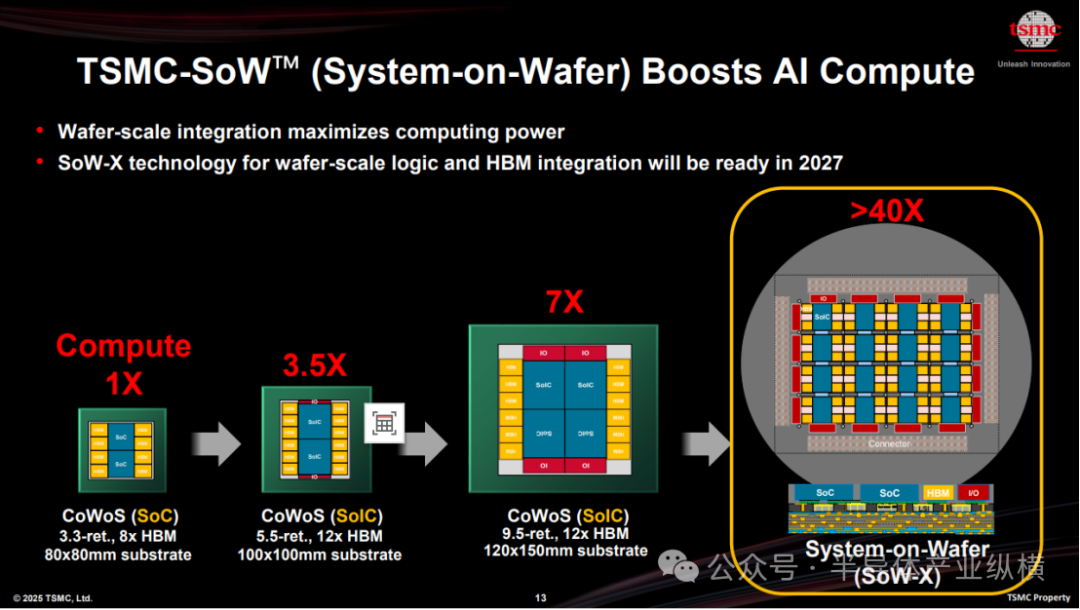
There's also the updated TSMC-SoW packaging, extending the integration scale to the wafer level. One approach is the pre-chip (SoW-P) method, where chips are placed on a wafer, and then integrated RDLs are constructed to connect the chips together. Another is the post-chip (SoW-X) method, where the interposer is first constructed at the wafer level, and then chips are placed on it. The last method enables designs 40 times larger than standard reticle sizes.
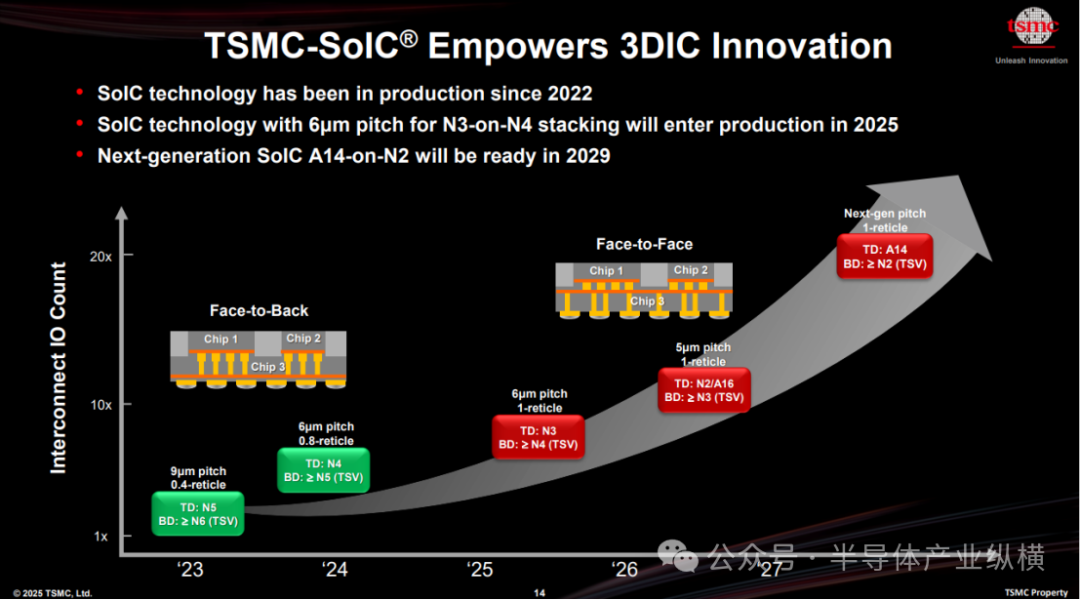
TSMC's SoIC technology plays a crucial role in extending Moore's Law. Instead of relying on traditional monolithic scaling, it adopts a chiplet-based architecture combined with high-density 3D heterogeneous integration. As one of the cornerstones of TSMC's 3DFabric platform, SoIC enables substrate-less 3D stacking, allowing dies of different nodes, functions, and materials to be vertically integrated through high-density interconnects.
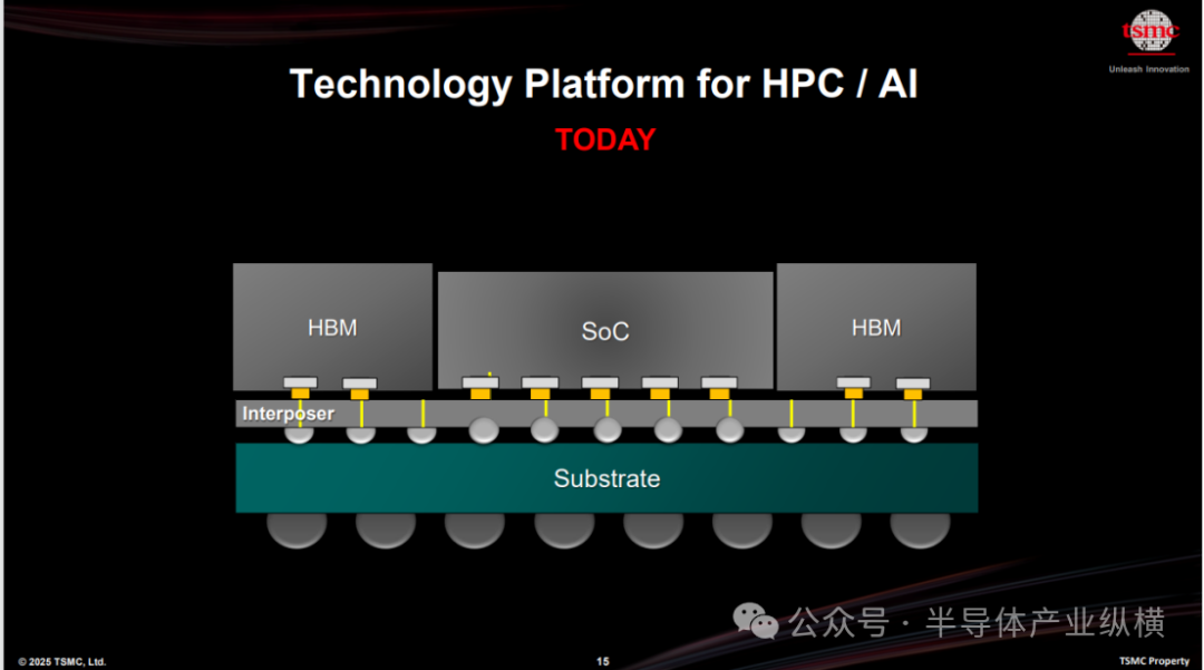
TSMC also showcased a typical AI accelerator application that integrates a monolithic SoC with an HBM memory stack through a silicon interposer.
TSMC introduced other high-performance integration solutions, including N12 and N3 process logic base dies for HBM4, and SiPh silicon photonics integration using COUPE compact universal photonic engine technology.
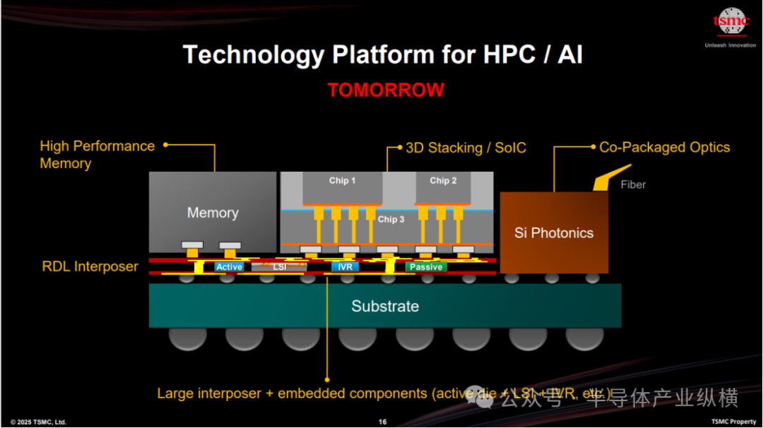
Regarding memory integration, TSMC emphasized the potential of CoW-SoW in combination with HBM4. With its ultra-wide 2048-bit interface, HBM4 is expected to address the urgent need for high-bandwidth, low-latency memory in AI and HPC workloads through tight integration with logic chips. This integration not only significantly boosts data transfer speeds but also effectively reduces power consumption.
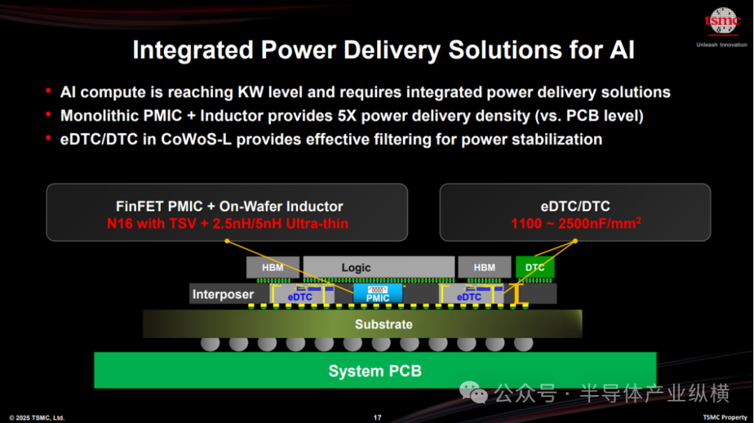
For power optimization, future AI accelerators may require several kilowatts of power, posing significant challenges for package-level power delivery. Integrated voltage regulators can help address these issues. TSMC has developed a high-density inductor, a critical component for such regulators. A monolithic PMIC combined with this inductor can provide 5 times the power delivery density compared to PCB-level solutions.
Many innovative applications also require advanced packaging technologies.
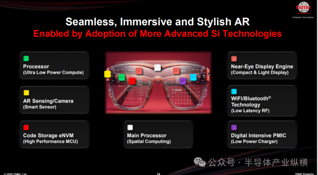
Augmented reality glasses serve as an example of a new product category requiring components like ultra-low-power processors, high-resolution cameras for AR perception, embedded non-volatile memory (eNVM) for code storage, large main processors for spatial computing, near-eye display engines, WiFi/Bluetooth for low-latency RF, and digital-intensive power management integrated circuits (PMICs) for low-power charging. This type of product will set new standards for complexity and efficiency.
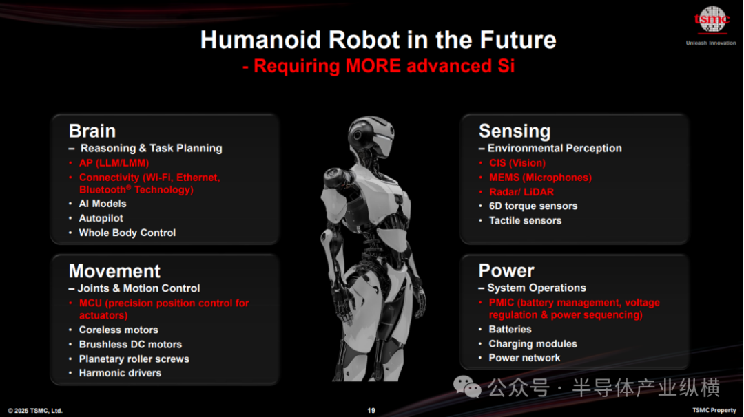
While autonomous vehicles receive significant attention, the demand for humanoid robots is also noteworthy. These robots require a substantial amount of advanced silicon, and the ability to integrate all these chips into high-density, energy-efficient packages is crucial.
-
![]()
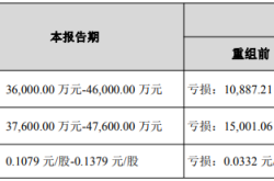
OFILM Reports Colossal 460 Million Yuan Loss: Founder Quietly Shifts Focus to Optical Modules!
-
![]()
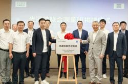
Yutong Optics and Zeiss Forge Partnership to Develop Quality Measurement System and Launch "Optical Communication Joint Measurement Class"
-
![]()
AutoNavi Revises Splash Screen Ads with Precision Amid Controversy
-
![]()
Unlicensed Vehicle Disputes: AutoNavi Ensnared in the Aggregation Model
-
![]()
Agent: The 'Hard Requirement' for Entering Core Enterprise Systems for the First Time
-
![]()
Global Auto Market Outlook: Sales Decline in China, US, and Europe, Chinese Exports Approach 10 Million
-
![]()
AI Pioneer Breaks Free from the 'Doldrums'
-
![]()
Valuation Exceeds $26 Billion! Three Chinese "Gold Medalists" Shake Up the AI Industry