3D-IC Tripartite Battle: Intel, TSMC, and Samsung's Vertical Breakthroughs
 05/09 2025
 892
892
Produced by Zhineng Zhixin
3D Integrated Circuits (3D-ICs) are emerging as the focal point of the next semiconductor competition. Amidst the surging demand for AI computing power, traditional planar SoCs struggle under the triple constraints of power consumption, performance, and cost, making chip stacking solutions pivotal to breaking this stalemate.
Intel, TSMC, and Samsung, the three industry titans, compete fiercely across various dimensions including materials, packaging, interconnection, heat dissipation, and EDA, striving to establish the technological foundation for the new era of AI chips. This article delves into the strategic layouts and pathway differences of these three foundry giants in 3D-ICs, exploring how they are tackling technical challenges one by one.
Part 1
Chips Enter the "Three-Dimensional Era": Why 3D-IC is Inevitable
For decades, the semiconductor industry has relied on Moore's Law for planar scaling, with each new node delivering performance enhancements and cost reductions. However, physical limitations and increasing manufacturing complexity have gradually eroded the benefits of advanced nodes. Especially in AI chips, which demand highly parallel and bandwidth-intensive computing, traditional SoCs face obstacles such as the "memory wall," "interconnection bottleneck," and "thermal limits."
3D-IC is not a novel concept; it has been on foundry roadmaps for over a decade. Yet, its progress remained sluggish until the recent surge in generative AI applications sparked by ChatGPT. Nowadays, AI chips necessitate tighter coupling of high-density computing and high-bandwidth memory, making chiplet architecture and advanced packaging prominent. 3D-IC has once again come into the spotlight, nearing the tipping point for large-scale commercialization.
Unlike simple 2.5D packaging, true 3D-IC requires:
- Multi-layer stacking for vertical integration of logic, cache, and memory
- Precision interconnection technologies like Hybrid Bonding for ultra-small pitch interconnections
- Innovative thermal management solutions such as thermal vias, vapor chambers, and microfluidic cooling
- New EDA methods supporting 3D layout, thermal simulation, and multi-physics modeling
- New supply chain integration involving collaboration from materials, tools to system vendors
These are not isolated technological breakthroughs but rather an ecosystem-wide transformation.
Part 2
Analysis of the "Verticalization" Roadmaps of the Three Giants: Competition and Differences Coexist
01
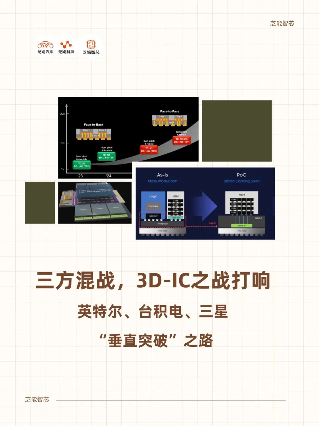
TSMC: Focusing on CoWoS and SoIC to Build a Hierarchical Packaging Ecosystem
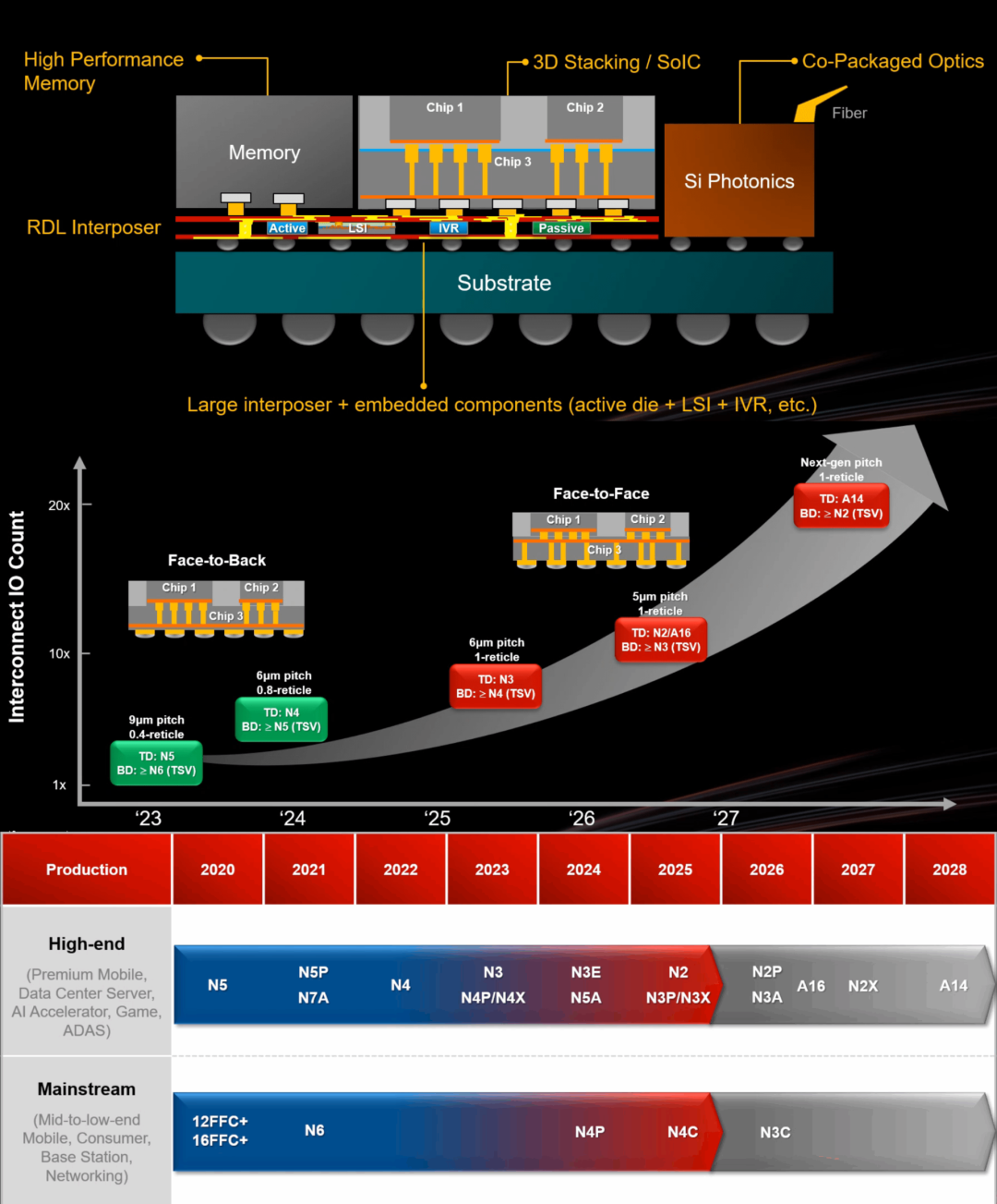
TSMC was the first foundry to establish mass production capabilities in 3D packaging. Its success stems from integrating advanced packaging into its main strategic line of parallel development with transistor technology. TSMC proposes a holistic solution for "system-level integration," encompassing:
- CoWoS (Chip-on-Wafer-on-Substrate): Focuses on 2.5D integration of high-bandwidth memory and logic chips
- SoIC (System on Integrated Chips): Develops face-to-face and face-to-back stacking technologies
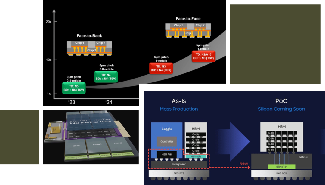
- Super Bonding Technology: Continuously reduces interconnection pitch, evolving from 9μm to 5μm
- Heterogeneous Integration Strategy: Supports not only advanced logic but also collaborative integration of N-1, N-2 node logic with high-density cache and analog circuits
TSMC emphasizes that transistor and packaging technologies must advance in tandem, aiming to tightly couple SRAM, HBM, and logic modules through dense stacking to resolve data flow bottlenecks and unleash the computational efficiency of AI chips.
02
Intel: Breakthroughs in System-Level Platform Integration under IDM 2.0
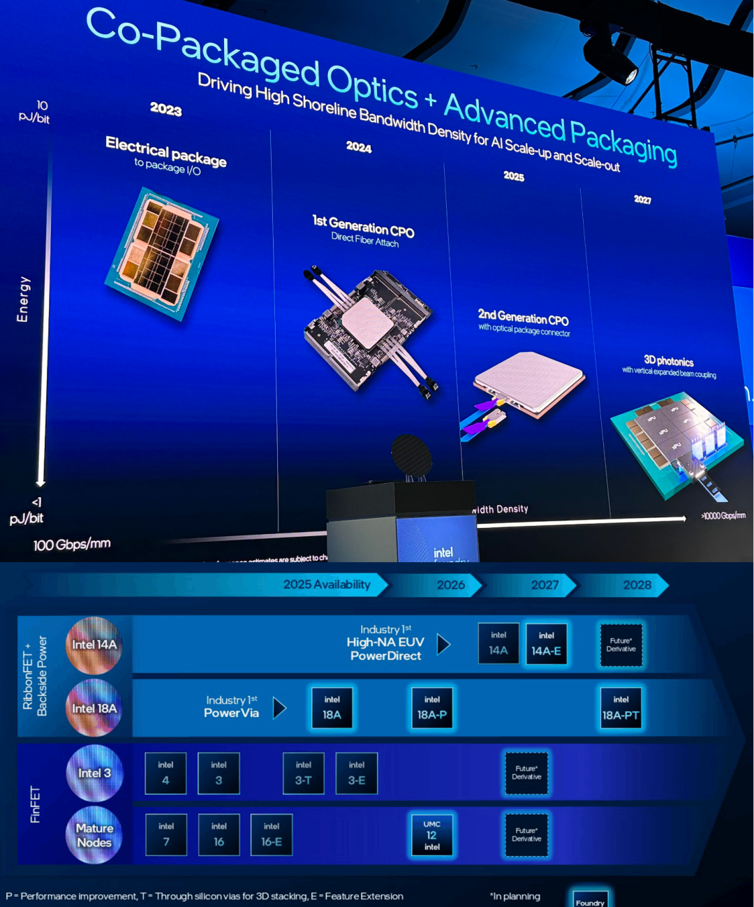
Intel's strength lies in its vertically integrated manufacturing system, encompassing EDA, design, packaging, and final testing. The introduced Foveros Direct technology emphasizes high-density stacking and vertical integration layout for SRAM. For instance:
- The 14A logic layer is directly stacked on top of the SRAM cache layer to maximize on-chip cache utilization
- Utilizes EMIB (Embedded Multi-die Interconnect Bridge) for horizontal connection of I/O and other computing components to optimize bandwidth
- Introduces AI-assisted EDA toolchains to enhance the designability and first-time success rate of 3D packaging
- Promotes the commercialization of the Logic-on-Logic architecture
Intel believes that constructing a stacked structure with "high cache + high bandwidth" is crucial for addressing the coordination bottleneck of AI cores' "compute-memory-bandwidth." This is also one of the strategies it is banking on to reclaim its position in the high-performance market.
03
Samsung: 3.5D Solution with LCOE+HBM+Foundry Collaborative Evolution
Samsung starts with the vertical integration capabilities of HBM and gradually progresses towards system-level stacking, emphasizing the collaborative design of logic and memory. Its roadmap outlines:
- LCOE (Logic-Centric Over-layering): Stacks SF2 and SF4X logic chips on another substrate to form a 3.5D integrated structure
- Plans to stack SF1.4 and SF2P at a higher level by 2027
- Customizes HBM to meet AI chip demands, even attempting to design exclusive HBM configurations for customers
- Places greater emphasis on collaboration with system vendors through joint design of customized packaging solutions
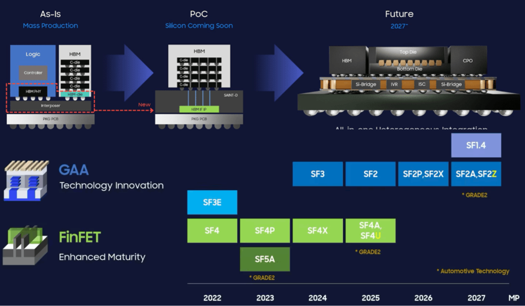
While Samsung's logic process slightly lags behind TSMC in advanced nodes, it has deep expertise in memory stacking and thermal management. Its 3D-IC strategy leans more towards the commercialization priority path of "AI memory-logic collaborative integration."
Heat dissipation, compared to interconnection and EDA toolchains, is the final hurdle impeding the true commercialization of 3D-IC. The three giants are advancing different thermal management technologies:
- TSV (Through-Silicon Via): Conducts heat through "mini chimneys," requiring dynamic optimization of TSV count and distribution based on workloads
- Vapor Chambers: Suitable for data center environments, utilizing phase change cooling, potentially replacing some air cooling
- Microfluidic Cooling: Embeds cooling channels within the chip to improve heat exchange efficiency, but manufacturing is complex and not yet scaled
The high power consumption of AI training chips necessitates collaborative design of hot and cold paths within the package, with EDA tools needing to support thermal modeling and dynamic workload simulation, posing significant challenges. 3D-IC is not merely a simple stacking of materials but a full-stack battle encompassing EDA, packaging, heat dissipation, testing, and design collaboration.
At this juncture, the entity that first establishes a vertical collaboration chain spanning design, manufacturing, packaging, and systems will gain the upper hand in the new era of AI chips.
TSMC emphasizes that packaging is the future node, Intel bets on cache stacking and system integration, and Samsung advances with the collaborative promotion of HBM and logic. Different paths lead to the same goal: building the next-generation "AI superchip platform."
Summary
The Next Stage of the 3D-IC War: A Competition of Systems, Not Just Technology
As 3D-IC vertical stacking becomes mainstream, victory is no longer determined by leadership in a single technology but by the overall system architecture and platform integration capabilities. In the future, chip manufacturing will not merely be a "battle of processes" but also a "battle of systems."
-
![]()
OFILM Reports Colossal 460 Million Yuan Loss: Founder Quietly Shifts Focus to Optical Modules!
-
![]()
Yutong Optics and Zeiss Forge Partnership to Develop Quality Measurement System and Launch "Optical Communication Joint Measurement Class"
-
![]()
AutoNavi Revises Splash Screen Ads with Precision Amid Controversy
-
![]()
Unlicensed Vehicle Disputes: AutoNavi Ensnared in the Aggregation Model
-
![]()
Agent: The 'Hard Requirement' for Entering Core Enterprise Systems for the First Time
-
![]()
Global Auto Market Outlook: Sales Decline in China, US, and Europe, Chinese Exports Approach 10 Million
-
![]()
AI Pioneer Breaks Free from the 'Doldrums'
-
![]()
Valuation Exceeds $26 Billion! Three Chinese "Gold Medalists" Shake Up the AI Industry