Unexpected Growth in the EDA Industry
 05/29 2025
 853
853
The ESD Alliance, a division of SEMI, has released its latest Electronic Design Market Data (EDMD) report, revealing a remarkable 11% year-on-year growth in EDA industry revenue, totaling $4.9 billion in Q4 2024. Despite a sluggish performance in the Chinese market, the global EDA industry has maintained a steady growth trajectory, with notable advancements in sub-sectors such as PCB design and packaging design.
The EDA sector is exhibiting unexpected growth trends.
01 Overall Performance of the Global EDA Industry
The EDA software industry is predominantly driven by technological advancements and characterized by high barriers in technology, talent, user collaboration, and capital. This has led to a highly concentrated market. For an extended period, the Chinese EDA market has been dominated by international giants Cadence, Synopsys, and Siemens EDA, with these top three companies holding over 70% of the market share.
What Drives EDA Growth?
Firstly, the burgeoning demand for edge computing and high-performance computing (HPC) chips has spurred the need for more sophisticated and automated EDA solutions.
Secondly, the increasing adoption of cloud-based solutions has emerged as a significant growth driver, facilitating seamless collaboration and enhancing accessibility for global design teams. Companies are increasingly integrating artificial intelligence (AI) and machine learning algorithms into their workflows to optimize design accuracy and efficiency, minimize costly errors, and expedite time-to-market.
Furthermore, the rise of domain-specific electronic product design and a heightened focus on energy-efficient chipsets for IoT and AI applications are anticipated to propel innovation in EDA solutions. Heightened R&D investment and strategic collaborations between semiconductor companies and EDA solution providers will further expand market potential.
By Product Category:
By Sub-sector:
Numerous companies are offering EDA solutions integrated with cutting-edge technologies such as AI and machine learning to alleviate the workload on design engineers. For instance, in July 2021, Cadence Design Systems launched the Cerebrus Intelligent Chip Explorer, a machine learning tool designed to automate the chip design process and enhance the efficiency of design engineers. Additionally, in December 2021, Nexar (a subsidiary of Altium Limited) collaborated with SnapEDA to enhance PCB design performance by providing computer-aided design (CAD) models and software, assisting engineers in designing electronic circuits more swiftly. Thus, the need to simplify integrated circuit design is fueling the demand for EDA solutions, thereby driving market growth.
02 AI Ushers in a New Era for EDA
EDA vendors now leverage AI technology to optimize EDA software engines, processes, and workflows. Crafting high-quality AI engines is crucial for achieving scalable and reliable results. AI algorithm models must be verifiable, accurate, and robust to ensure safety across the enterprise and consistently deliver sustainable outcomes.
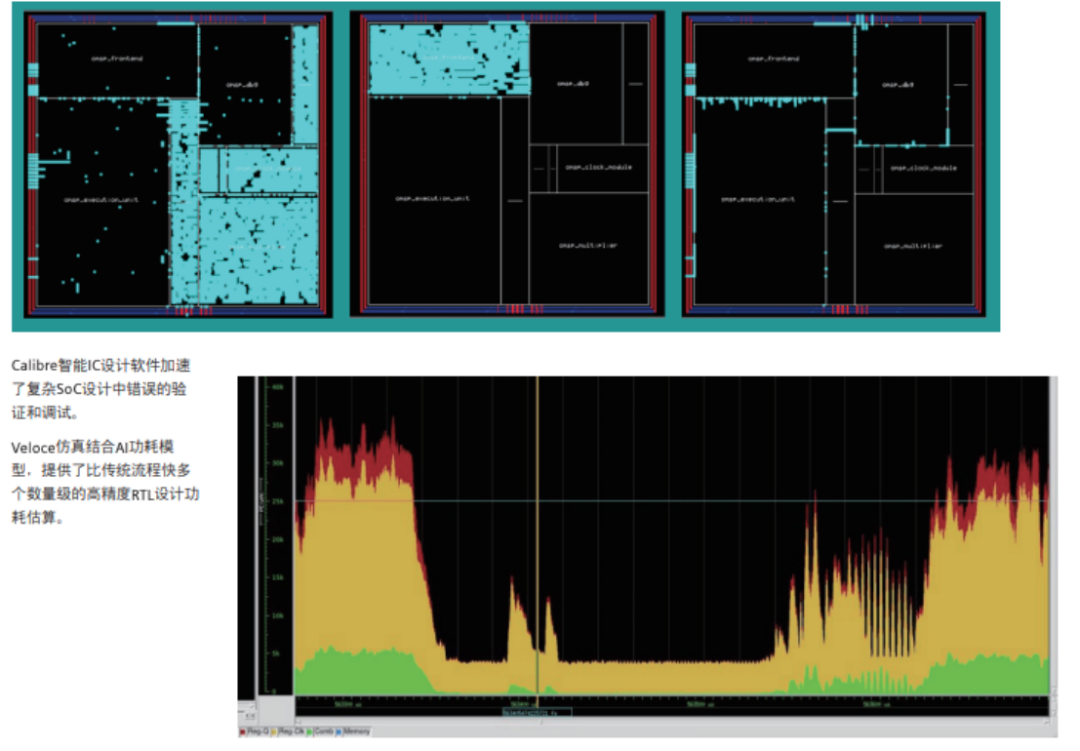
In Siemens EDA solutions, AI technology is applied in three key areas: core technology, process optimization, and providing a scalable open platform. Its primary applications revolve around enhancing engineers' capabilities, improving productivity, and capturing knowledge within design teams. AI provides insights into IC design, aiding in understanding the root causes of issues and preventing potential problems in the future. The ability to automate with AI and verify AI results is paramount. Verifiability, traceability, and openness are core requirements for AI in EDA applications. In AI-enabled Siemens EDA solutions, the verifiable engine is built on the foundation of accuracy, robustness, domain expertise, and usability, ensuring that AI algorithms deliver predictable, repeatable, and valuable results when processing data. In cases where verification cannot be automated, expertise is required to assess and ensure the correctness of results. With over a decade of continuous improvement and market success, Siemens EDA deeply understands the prerequisites for extending a credible and verifiable AI platform.
The application of AI in EDA tools can be categorized into several key aspects. Firstly, it handles heavy, repetitive tasks. The chip design process involves numerous stages requiring repeated verification and optimization, such as power consumption simulation, thermal distribution analysis, and logic verification. Traditional methods often necessitate engineers to spend weeks or even months making adjustments, whereas AI algorithms can accomplish these tasks in a shorter time with greater accuracy. For example, Synopsys' suite of AI-driven EDA tools can swiftly handle tasks from system architecture definition to design implementation, verification, and manufacturing. This significantly shortens the design cycle and reduces the demand for engineers.
Secondly, AI demonstrates robust optimization capabilities in chip design. Google's AlphaChip serves as an illustration; this AI tool based on reinforcement learning achieves "superhuman" performance in chip layout design. By learning from data from previous generations of chip designs, AlphaChip can rapidly generate complex chip layout schemes, compressing work that traditional designers would take weeks to complete into just a few hours. More importantly, AI-generated design schemes often strike a better balance in terms of performance, power consumption, and heat dissipation. Google's Tensor Processing Units (TPUs) are a prime example where each generation's design benefits from optimization by AI tools.
Moreover, generative AI (GenAI) is beginning to make its mark in EDA tools. Unlike traditional AI technologies, GenAI functions more like an intelligent assistant capable of generating new design schemes or providing design suggestions by learning from existing data. For instance, Synopsys' GenAI technology can quickly scan chip design specification documents up to hundreds of pages long and extract key information for designers' reference. This capability not only enhances design efficiency but also reduces the cognitive burden on designers tackling complex projects. More intriguingly, GenAI can also assist with tasks such as code optimization and verification constraint extraction, providing designers with more instructive advice.
However, AI-driven EDA tools are not devoid of limitations. The current biggest challenge lies in data availability. Each chip design company possesses its proprietary intellectual property and design data, which are typically not shared. This implies that AI tools can only be trained on limited data, making it challenging to achieve generalized design across companies or domains. Additionally, the application of AI in chip design is still in its nascent stages, and while the ambition of fully relying on AI for end-to-end design is exciting, it is still some distance from being realized.

User Comments
03 Future Outlook
As the semiconductor industry enters the post-Moore era, the emergence of Chiplet technology is profoundly transforming the paradigm of chip design and manufacturing. This technological approach, which involves decomposing a large single SoC into multiple small chips and then integrating them through advanced packaging, not only continues the path of performance improvement but also presents new demands on the EDA tool chain.
Traditional EDA tools are primarily focused on the front-end and back-end design processes of a single chip, whereas Chiplet technology requires tools to support collaborative optimization across the entire process, from chip decomposition during architecture exploration and interconnect topology design to signal integrity analysis and thermal simulation at the packaging level. This necessitates EDA vendors to restructure their tool architectures and develop new platforms that support heterogeneous integrated design. Represented by Synopsys' 3DIC Compiler and Cadence's Integrity 3D-IC platform, the industry has witnessed the advent of tool suites specifically tailored for Chiplet design, which need to address new challenges such as silicon interposer routing, micro-bump array optimization, and cross-die clock synchronization. Notably, the market size of packaging tools is transitioning from a supporting role to a critical path, with Yole predicting that the advanced packaging EDA market will surpass $500 million by 2025, exhibiting a significantly higher compound annual growth rate than traditional EDA tools.
From a technological evolution perspective, the collaborative design capabilities of EDA tools and IPs will be crucial for competition. EDA vendors' IP businesses still heavily rely on royalty income from traditional interface protocols (such as USB, PCIe), and these standardized IPs are gradually becoming a red ocean market. A case in point is the rise of the RISC-V ecosystem, which has expanded the overall size of the processor IP market, but the main beneficiaries have been emerging companies like SiFive rather than the traditional EDA giants. This differentiation trend suggests that EDA vendors may need to reassess their IP strategies, deciding whether to concentrate resources on the in-depth development of specific high-performance IPs or broaden their IP portfolios through mergers and acquisitions.
Data from TSMC's 3DFabric Alliance indicates that customers adopting Chiplet designs need to integrate IP modules from an average of 8-12 different suppliers, placing high demands on the unified interface and verification processes of design tools. Leading EDA vendors have commenced building fully integrated platforms for "design-verification-packaging," such as Cadence's Cerebrus intelligent chip design system, which can automatically optimize Chiplet layout and interconnect solutions. However, the challenge lies in the exponential growth of the design space with increasing Chiplet heterogeneous integration, rendering traditional simulation methods inadequate. This explains why major vendors are accelerating their deployment of AI-driven design tools, with Synopsys' DSO.ai and Cadence's JedAI platforms aiming to tackle the complexity of Chiplet collaborative optimization using machine learning algorithms. In the next five years, EDA platforms that can provide comprehensive solutions from architecture exploration to physical implementation will gain greater influence in the Chiplet era.
-
![]()
OFILM Reports Colossal 460 Million Yuan Loss: Founder Quietly Shifts Focus to Optical Modules!
-
![]()
Yutong Optics and Zeiss Forge Partnership to Develop Quality Measurement System and Launch "Optical Communication Joint Measurement Class"
-
![]()
AutoNavi Revises Splash Screen Ads with Precision Amid Controversy
-
![]()
Unlicensed Vehicle Disputes: AutoNavi Ensnared in the Aggregation Model
-
![]()
Agent: The 'Hard Requirement' for Entering Core Enterprise Systems for the First Time
-
![]()
Global Auto Market Outlook: Sales Decline in China, US, and Europe, Chinese Exports Approach 10 Million
-
![]()
AI Pioneer Breaks Free from the 'Doldrums'
-
![]()
Valuation Exceeds $26 Billion! Three Chinese "Gold Medalists" Shake Up the AI Industry