Lightmatter's Passage M1000: Revolutionizing Photonic Interconnect Technology | HotChips 2025
 09/04 2025
 798
798
Produced by Zhineng Zhixin
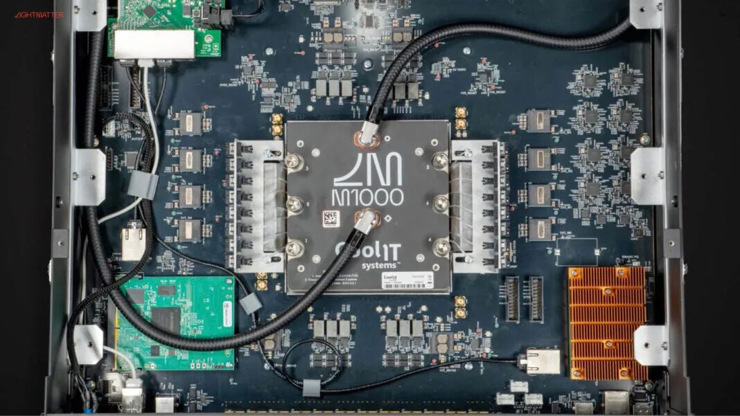
At the Hot Chips 2025 conference, Lightmatter unveiled its groundbreaking optical interconnect platform, the Passage M1000. Leveraging silicon photonics technology, this innovative product achieves a bidirectional communication bandwidth of up to 114Tbps for computing and memory chips by seamlessly integrating optical I/O into the interposer layer.
What's particularly fascinating is its ability to transcend traditional electrical interconnect limitations at the package boundary. Through advanced technologies such as microring modulators, 16-wavelength lasers, and reconfigurable optical path switching, the Passage M1000 showcases the unparalleled advantages of optical communication in chiplet-based computing architectures.
Part 1: Lightmatter's Technological Implementation Path
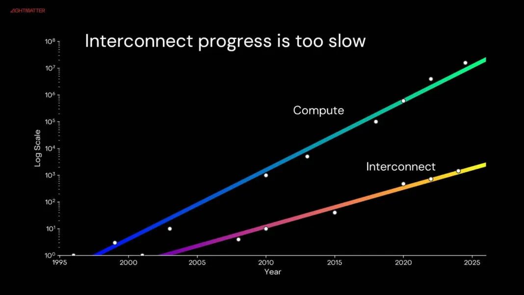
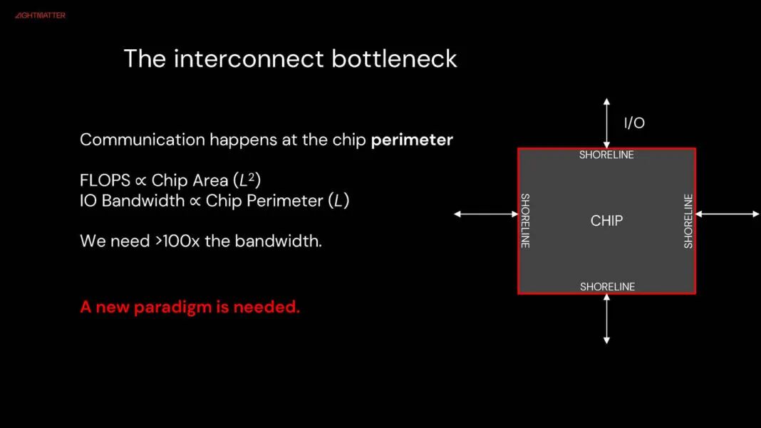
The rapid scaling of computing systems is increasingly hindered by interconnect bottlenecks. As computational demands from GPUs, AI accelerators, and XPUs surge exponentially, traditional SerDes solutions, despite continuous evolution, are approaching their limits in pin density and power consumption at the package perimeter.
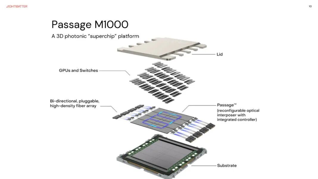
The Passage M1000 addresses this challenge by embedding optical I/O directly into the package interposer layer, enabling close-proximity integration of computing chips, memory chips, and optical devices.
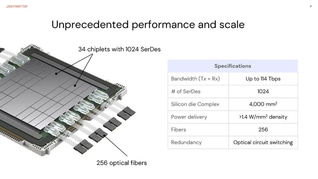
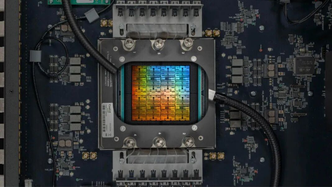
Architecturally, the core of the Passage M1000 lies in its optical interposer layer. On this layer, computing chips and memory chips can be co-packaged, with data generating and modulating optical signals through microring modulators, which are then efficiently transmitted via a 16-wavelength laser-based wavelength division multiplexing system.
Compared to electrical interconnects, optical links offer higher bandwidth density, lower loss, and extended reach. This enables the M1000 to deliver a total bandwidth of 114Tbps (57Tbps in each direction), paving the way for future 200Tbps-class XPUs and 400Tbps-class switches.
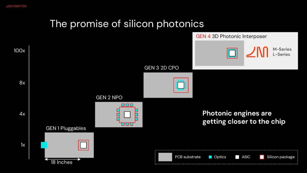
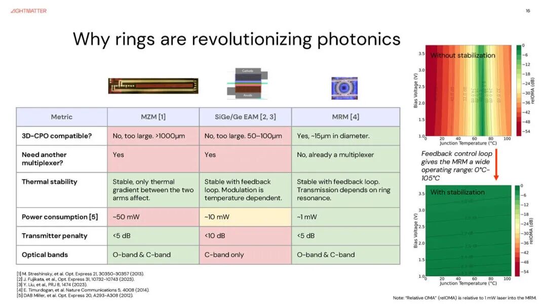
At the device level, Lightmatter employs silicon microrings as modulation elements. Unlike common electro-absorption modulators (EAMs), microrings offer a more compact structure, allowing for the integration of more channels within a limited package area, thus increasing I/O density.
To address the mismatch between optical component sizes and electrical SerDes, the M1000 achieves a compact package through 3D stacking and incorporates a liquid cooling solution (CoolIT cooler) to manage thermal loads under high-bandwidth operations.
Moreover, the M1000's optical paths offer a degree of reconfigurability. Its switching network can dynamically allocate links and perform redundant switching in case of failure, resembling a self-healing optical network layer that ensures high-reliability operations in large-scale data centers and AI clusters.
Part 2: From Technology Prototype to Scale Deployment
At Hot Chips 2025, Lightmatter was not alone in pushing the boundaries of photonic interconnects. Vendors like Celestial AI proposed different optical modulation approaches (such as EAMs), highlighting the industry's ongoing quest for the optimal balance between performance, power consumption, and cost.
While Lightmatter's microring solution is compact, it still faces challenges related to temperature drift and manufacturing complexity. The market is expected to witness the parallel evolution of multiple technologies, with the optimal solution ultimately determined by specific application scenarios.
Despite its compatibility with large-scale CMOS processes, silicon photonics technology still grapples with high costs in light sources, waveguide coupling, precision packaging, and other aspects. Notably, the M1000's 16-wavelength lasers and multi-channel microrings require stringent process consistency and temperature stability to avoid signal distortion and increased energy consumption.
The key to transitioning photonic interconnects from the lab to mass production while maintaining performance lies in achieving high yield. Currently, mainstream GPUs, CPUs, and XPUs primarily rely on electrical SerDes for interconnectivity. The Passage M1000, therefore, needs to interface with these devices through SerDes and convert signals to optical format, adding complexity to the system during this transitional period.
To fully harness the benefits of optical interconnects in the future, computing chip manufacturers must adopt photonic packaging solutions more deeply. This transition necessitates the co-evolution of standardized interfaces, EDA toolchains, and supply chains.
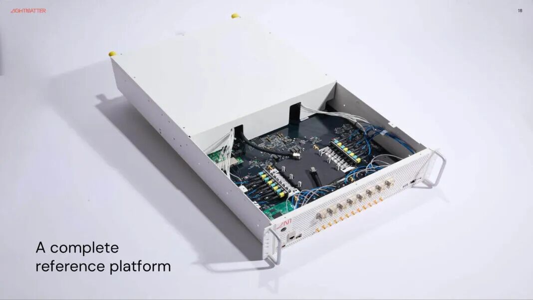
While Lightmatter has already showcased a reference platform, the journey from single-machine demonstrations to large-scale deployment in cloud data centers is fraught with challenges. This includes extensive validation cycles for long-term stability, power consumption performance under various application loads, and compatibility with existing network switches.
Broadcom's Tomahawk 6 offers 102.4Tbps switching capability, whereas the M1000 aims for the 400Tbps level. It will take time to validate whether optical solutions can indeed become a viable alternative in the high-end switching market.
Conclusion
By integrating optical devices into the interposer layer, Lightmatter's Passage M1000 elevates bandwidth density to hundreds of Tbps, laying the groundwork for future system architectures that will demand similarly high bandwidth levels. The Passage M1000 represents a bold attempt to rebalance computing power and bandwidth, heralding a new era in high-performance computing and data communication.
-
![]()
The Surprisingly Significant Impact Difference Between Quiet and Noisy Cars!
-
![]()
Breaking Through Storage Cycle Barriers: How AI Large Models and Coding Technology Synergize to Drive Transformation in the Security Industry
-
Facilitating the Slimming of Camera Modules! O-film Obtains Utility Model Patent for Periscope-Type Reflective Component
-
![]()
Hikvision Raytine’s Millimeter-Wave Body Imaging Security Inspection Device Achieves ECAC SSc Category A Standard Level 2.1 Certification for European Civil Aviation
-
![]()
Global Market Share for Security Windows Hits 26%! This Optical 'Little Giant' Makes Its Debut on NEEQ
-
![]()
The Evolutionary Path of Agent Engineering: From Prompt to Harness by Zhang Yutao, Co-founder of Moonshot AI
-
![]()
Profits and stock prices are both declining, so why are executives from these auto companies increasing their purchases?
-
![]()
Burning Tens of Billions of Dollars, Yet No Unified Definition for World Models