Wafer-scale Chips: The Future of High-Performance Computing
 06/30 2025
 825
825

Today, large AI model parameters are soaring into the billions.
In just two years, the computational demands of these models have skyrocketed, increasing by a factor of 1,000, far outpacing the pace of hardware advancements. Currently, the mainstay solution for supporting these large AI models relies heavily on GPU clusters.
However, the limitations of single-chip GPUs are evident: Firstly, the physical size of a single chip constrains the number of transistors it can house, and even with advanced manufacturing processes, performance enhancements are nearing the limits prescribed by Moore's Law. Secondly, when interconnecting multiple chips, latency and bandwidth loss during data transmission between chips prevent the overall performance from scaling linearly with the number of chips.
This is why, when confronted with trillion-parameter models like GPT-4 and ERNIE Bot, even the aggregation of thousands of NVIDIA H100s fails to escape the dilemma of "insufficient computational power and exorbitant electricity bills".
Currently, the AI training hardware industry is polarized into two distinct camps: dedicated accelerators leveraging wafer-scale integration technology (such as Cerebras WSE-3 and Tesla Dojo) and GPU clusters based on traditional architectures (like NVIDIA H100).
Wafer-scale chips are widely regarded as the next frontier in high-performance computing.
01
Wafer-scale Chips: Two Major Players
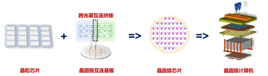
In the conventional chip production process, a wafer undergoes photolithography and is subsequently diced into many individual dies, each of which is encapsulated separately. After encapsulation, each die becomes a complete chip.
The conventional approach to enhancing chip computational power involves increasing the chip area. As such, chip manufacturers are constantly striving to do just that. Currently, the die size of computing power chips is approximately 26x33=858mm², nearing the size of the exposure window, but the maximum chip size cannot exceed the exposure window size.
The size of the exposure window has remained stagnant for many years, becoming one of the key constraints hindering the growth of chip computational power.
Wafer-scale chips offer an innovative alternative. By manufacturing a wafer-scale interconnect substrate without dicing and then integrating and encapsulating the designed conventional dies onto this wafer substrate, a single, massive chip is produced.
The circuit units and metal interconnects on an uncut wafer are arranged more tightly, forming an interconnect structure with higher bandwidth and lower latency. This effectively constructs larger computational power nodes through high-performance interconnects and high-density integration. As a result, under the same computational power, the footprint of a computing cluster built with wafer-scale chips can be reduced by more than 10-20 times compared to a GPU cluster, with power consumption decreased by more than 30%.
Globally, two companies have developed wafer-scale chip products.
One is Cerebras. Established in 2015, the company launched the WES-1 in 2019 and has since iterated to the third-generation wafer-scale chip, the WES-3.
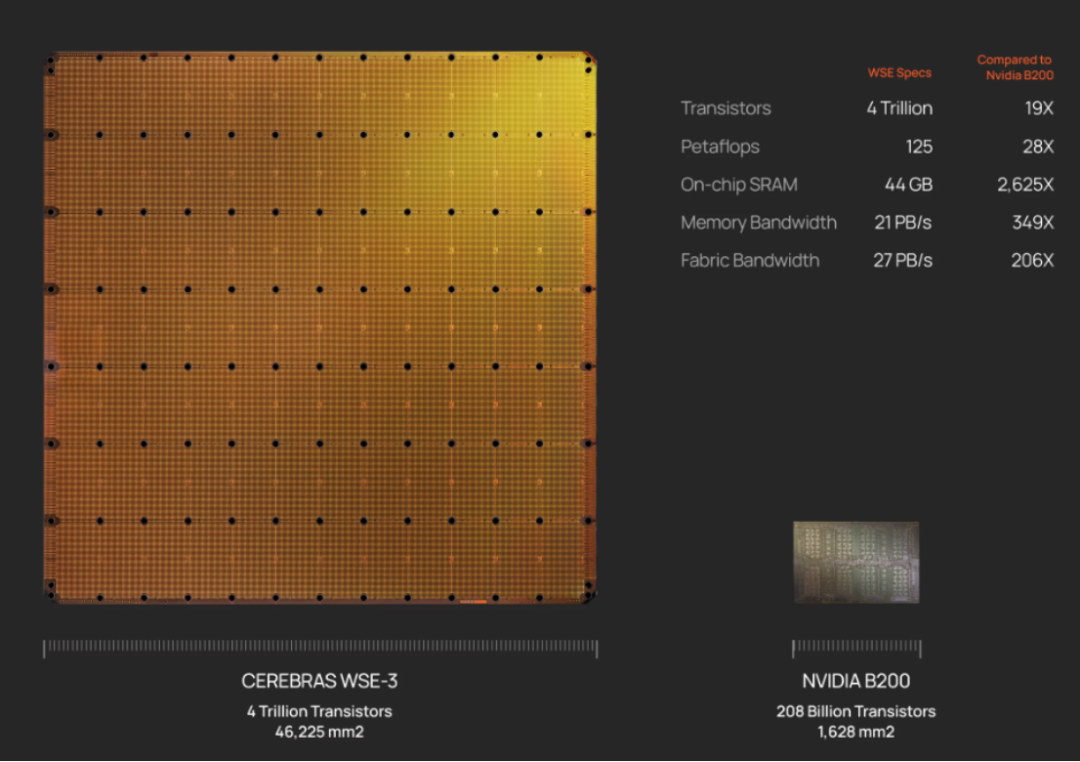
The WES-3 utilizes TSMC's 5nm process, boasts an astonishing 4 trillion transistors, has increased the number of AI cores to 900,000, and offers a cache capacity of 44GB, supporting up to 1.2PB of off-chip memory.
The WES-3's capabilities enable the training of next-generation frontier large models that are 10 times larger than GPT-4 and Gemini. In a four-chip parallel configuration, it can complete the tuning of a 70 billion-parameter model within a day, supporting up to 2048 interconnects and finishing the training of a 70 billion-parameter Llama model in a day.
All this is seamlessly integrated onto a single 215mm×215mm=46,225mm² wafer.
To put this into perspective, compare it to the NVIDIA H100: The WES-3's on-chip memory capacity is 880 times that of the H100, its single-chip memory bandwidth is 7000 times that of the H100, its core count is 52 times that of the H100, and its on-chip interconnect bandwidth speed is 3715 times that of the H100.
The other company is Tesla. Tesla's wafer-scale chip is named Dojo. This initiative was spearheaded by Musk in 2021.
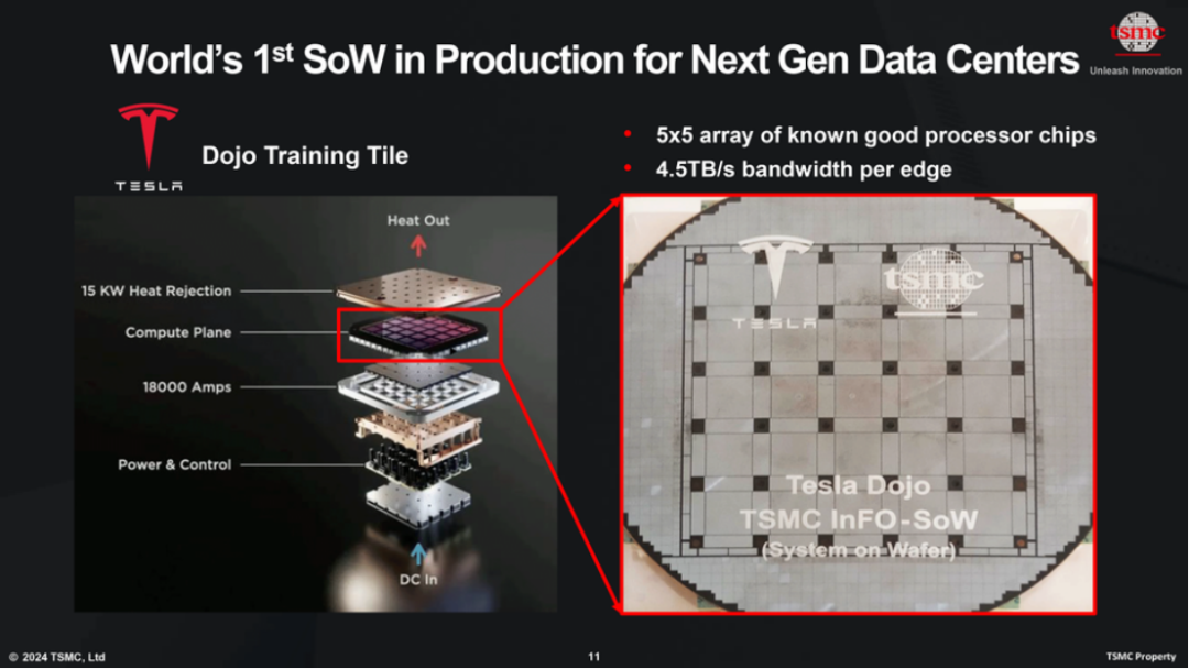
Tesla's Dojo adopts a different technical approach from Cerebras. It utilizes a chiplet route, integrating 25 proprietary D1 chiplets (dies) onto a wafer-sized substrate.
The D1 chiplet places 50 billion transistors on a 645mm² chip, with each chiplet providing 362 TFlops of BF16/CFP8 computational power. Collectively, a single Dojo boasts 9 Petaflops of computational power and 36TB of bandwidth per second.
Tesla's Dojo system is tailored specifically for the training needs of full self-driving (FSD) models. The approach starts with 25 D1 chiplets, forming a Training Tile, which is then combined into a Tray with 6 Training Tiles. Two Trays form a Cabinet, and 10 Cabinets make up an ExaPOD supercomputing system capable of delivering 1.1 EFlops of computational performance.
02
Comparison between Wafer-scale Chips and GPUs
Since single-chip GPUs and wafer-scale chips have taken divergent paths, let's compare the different explorations of these two chip architectures in pushing the limits of computational power, using Cerebras WSE-3, Dojo, and NVIDIA H100 as examples.
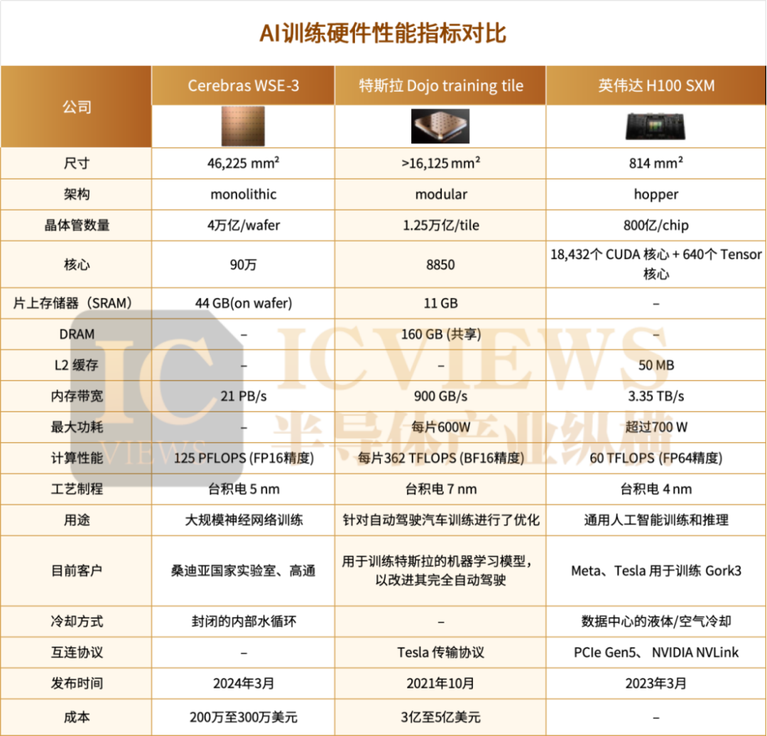
Generally, the performance of AI training chip GPUs is evaluated through several key indicators: Floating-point operations per second (FLOPS), indicating the raw computational power of GPUs in the matrix-intensive operations essential for deep learning; Memory bandwidth, determining the speed of accessing and processing data, directly affecting training efficiency; Latency and throughput, assessing the efficiency of GPUs in handling large data loads and model parallelism, thereby impacting real-time performance.
Computational Performance
Cerebras WSE-3 demonstrates unique potential in AI model training with its monolithic architecture.
FLOPS (Floating-point operations per second) generally indicates the raw computational power of GPUs in matrix-intensive operations crucial for deep learning. The WSE-3 achieves a peak FP16 training performance of 125 PFLOPS, supporting the training of AI models with up to 24 trillion parameters without the need for model partitioning. This feature is particularly well-suited for handling ultra-large models in a streamlined and efficient manner.
Unlike traditional GPUs that rely on a hierarchical memory architecture (which can create processing bottlenecks), WSE's design allows 850 cores to operate independently and directly access local memory, effectively enhancing computational throughput.
In contrast, NVIDIA H100 adopts a modular and distributed approach. A single H100 GPU provides 60 TFLOPS of FP64 computational power for high-performance computing, and a system of eight interconnected H100 GPUs can achieve over 1 ExaFLOP of FP8 AI performance.
However, distributed architectures present data transmission issues. Although NVLink and HBM3 memory can reduce latency, inter-GPU communication can still impede training speed when training ultra-large models.
In terms of AI training performance, Cerebras WSE-3 excels at handling ultra-large models. A cluster of 2048 WSE-3 systems can train Meta's 70 billion-parameter Llama 2 LLM in just one day, representing a 30-fold speed increase compared to Meta's original AI training cluster.
Latency and Throughput
From a data transmission perspective, WSE-3's monolithic architecture eliminates the need for data transmission between multiple chips, significantly reducing latency and supporting large-scale parallel computing and low-latency communication between cores. Speed is a monolithic advantage, with WSE-3 reducing software complexity by up to 90% compared to traditional GPU clusters, while also decreasing latency for real-time GenAI inference by more than 10 times.
Tesla's Dojo Training Tile, being wafer-scale integrated, can also significantly reduce communication overhead. Since data transfer occurs from die to die, there is still some latency when scaling across blocks. Currently, Dojo achieves 100 nanoseconds of inter-chip latency and optimizes throughput for autonomous driving training, capable of simultaneously processing 1 million video streams at 36 frames per second.
NVIDIA's H100, based on the Hopper architecture, is one of the most powerful AI training GPUs currently available, equipped with 18,432 CUDA cores and 640 tensor cores, and enabling high-speed communication between GPUs through the NVLink and NVSwitch systems. Although the multi-GPU architecture offers good scalability, data transmission introduces latency issues. Even with NVLink 4.0 providing 900 GB/s of bidirectional bandwidth per GPU, the latency is still higher than that of wafer-scale systems.
While capable of achieving low latency and high throughput for single-wafer workloads due to their architectural characteristics, wafer-scale systems like WSE-3 and Dojo face challenges of limited scalability, high manufacturing costs, and insufficient flexibility for general workloads.
Cost-Effectiveness
In terms of hardware acquisition costs, prices vary for different chips due to their architectures and application scenarios.
It is reported that the specific cost of a single Tesla Dojo supercomputer is estimated to be between $300 million and $500 million. Technologically, Dojo employs mature wafer processes combined with advanced packaging (using TSMC's Info_SoW technology integration) to achieve wafer-scale computational power, avoiding the challenge of pushing process limits. This not only ensures a higher yield rate but also facilitates large-scale production of systems, making it easier to update and iterate chiplets.
The Cerebras WSE system, on the other hand, faces higher initial R&D and production costs due to its advanced manufacturing processes and complex design. It is reported that the cost of each Cerebras WSE-2 system ranges from $2 million to $3 million.
In comparison, the procurement cost of a single NVIDIA GPU is relatively low. For NVIDIA A100, the 40GB PCIe model costs approximately $8,000 - $10,000, while the 80GB SXM model costs $18,000 - $20,000. This makes many enterprises initially more inclined to choose NVIDIA GPUs when building AI computing infrastructure. However, long-term use of NVIDIA GPUs can lead to increasing operational costs due to issues such as high energy consumption and performance bottlenecks in multi-chip collaboration.
Overall, while WSE-2 can provide ultra-high computational density for ultra-large-scale AI models, the cost advantage of A100 is more pronounced for organizations that need to deploy multi-GPU scalable solutions in large data centers and cloud services.
03
Conclusion
In conventional forms, the more computational power nodes a cluster has, the larger the cluster's scale, the greater the communication overhead, and the lower the cluster's efficiency.
This is why NVIDIA's NVL72 enhances computational density within the cluster (i.e., increases computational power density) by increasing the node integration density. By integrating far more GPUs than conventional racks into a single rack, the cluster's size is controlled, enabling further efficiency improvements.
This is a solution offered by NVIDIA after weighing yield rates and costs. However, if NVIDIA continues down this computational path and aims to further enhance computational power density, it will inevitably lead to the adoption of wafer-scale chips. After all, the form factor of wafer-scale chips offers the highest integration density of computational power nodes to date.
Wafer-scale chips hold limitless potential, poised to revolutionize the landscape of high-performance computing.
-
![]()
OFILM Reports Colossal 460 Million Yuan Loss: Founder Quietly Shifts Focus to Optical Modules!
-
![]()
Yutong Optics and Zeiss Forge Partnership to Develop Quality Measurement System and Launch "Optical Communication Joint Measurement Class"
-
![]()
AutoNavi Revises Splash Screen Ads with Precision Amid Controversy
-
![]()
Unlicensed Vehicle Disputes: AutoNavi Ensnared in the Aggregation Model
-
![]()
Agent: The 'Hard Requirement' for Entering Core Enterprise Systems for the First Time
-
![]()
Global Auto Market Outlook: Sales Decline in China, US, and Europe, Chinese Exports Approach 10 Million
-
![]()
AI Pioneer Breaks Free from the 'Doldrums'
-
![]()
Valuation Exceeds $26 Billion! Three Chinese "Gold Medalists" Shake Up the AI Industry