Match Rate Exceeds 99.7%! This Optical Enterprise Secures Nearly 100 Million Yuan in Exclusive Investment
 04/01 2026
 541
541
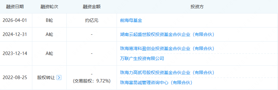
On April 1, Zhuhai Chengfeng Electronic Technology Co., Ltd. (hereinafter referred to as "Chengfeng Technology") announced the completion of nearly 100 million yuan in Series B financing, exclusively invested by Qianhai Fangzhou.
The financing news of this national-level specialized, refined, and innovative "Little Giant" enterprise has once again brought the process of domestic substitution of semiconductor optical inspection equipment into the spotlight. On a track where high-end equipment has long been monopolized by foreign giants, why has Chengfeng Technology won the favor of capital?
Founded in 2015 and headquartered in Zhuhai High-Tech Zone, Chengfeng Technology has accumulated over a decade of technical expertise in semiconductor optical inspection. Its core team consists of senior experts in optics, algorithms, and semiconductor processes, with an average industry experience exceeding 15 years. This composite background of "technology + industry" has laid a solid foundation for tackling core technical challenges.
Unlike many peers who chose to start with relatively simple appearance inspections, Chengfeng Technology aimed from the outset at the most challenging field of pattern inspection—a technical frontier requiring the identification of minute abnormalities in microscopic circuits on wafers. Moreover, the company chose the most difficult yet most valuable path: full-stack self-research.
After years of dedicated research, Chengfeng Technology independently developed multiple sets of optical microscopic imaging technologies and mastered core pattern inspection algorithms. It successfully overcame key technologies for nanoscale wafer and photomask pattern inspections, accumulating over 60 national patents and breaking foreign technical blockades and market monopolies.

The ultimate validation of technical strength lies in the market. Currently, Chengfeng Technology's products form a matrix covering the entire semiconductor front-end and back-end processes, including multiple mass-produced models such as the CFW920/820 wafer inspection series, CFY210/401/501 photomask inspection series, and CF91X optical module inspection series. In the front-end manufacturing sector, the CFW820 microscopic pattern inspection equipment has completed comprehensive benchmark testing at China's top three wafer foundries, achieving a flaw detection rate match (Match Rate) exceeding 99.7% and throughput comparable to foreign competitors.
In the back-end sector, the CF91X series can be applied for precision inspections of 400G/800G/1.6T optical modules, further expanding market boundaries. These products have been mass-applied in leading domestic wafer foundries, photomask factories, and optical module enterprises, successfully replacing imported equipment and significantly reducing industrial chain (industrial chain) costs.
Capacity construction is key to measuring whether an equipment enterprise can achieve scalable development. In May 2025, Chengfeng Technology's semiconductor inspection equipment R&D and production base, invested in Ningxiang Economic Development Zone, Hunan, officially commenced operations. With a total investment of 500 million yuan, the project features a hundred-level high-standard cleanroom, focusing on the R&D and production of photomask inspection equipment.
The completion of this base not only fills the gap in Hunan's semiconductor inspection equipment sector but also provides the company with strong mass-production delivery capabilities—anticipated to achieve an annual output value of 1 billion yuan upon full capacity.
In terms of market layout, Chengfeng Technology has established R&D centers and production bases in Zhuhai, Changsha, Suzhou, Wuxi, Singapore, and other locations, extending its service network from the Greater Bay Area and Yangtze River Delta to overseas markets such as Thailand and Singapore.
The company adopts a strategy of "following existing customers overseas." As some clients set up factories in Southeast Asia, Chengfeng Technology's equipment go with the flow (naturally) enters local markets. This pragmatic internationalization path has made it one of the few domestic semiconductor inspection equipment enterprises capable of competing with international giants on the same stage.
On the technical front, the company is already exploring AI-driven inspection algorithms as a supplement to its existing mature algorithms, collaboratively enhancing inspection efficiency. This strategic determination to balance pragmatism with ambition may precisely be the underlying reason why Chengfeng Technology has secured favor against the odds during the capital winter.
With the infusion of nearly 100 million yuan in Series B funding, this "Little Giant" in the optical inspection field will continue to focus on core technology iteration, production line expansion, and market expansion, contributing solid strength to China's self-controlled semiconductor industrial chain. The future looks promising.
-
![]()
The Surprisingly Significant Impact Difference Between Quiet and Noisy Cars!
-
![]()
Breaking Through Storage Cycle Barriers: How AI Large Models and Coding Technology Synergize to Drive Transformation in the Security Industry
-
Facilitating the Slimming of Camera Modules! O-film Obtains Utility Model Patent for Periscope-Type Reflective Component
-
![]()
Hikvision Raytine’s Millimeter-Wave Body Imaging Security Inspection Device Achieves ECAC SSc Category A Standard Level 2.1 Certification for European Civil Aviation
-
![]()
Global Market Share for Security Windows Hits 26%! This Optical 'Little Giant' Makes Its Debut on NEEQ
-
![]()
The Evolutionary Path of Agent Engineering: From Prompt to Harness by Zhang Yutao, Co-founder of Moonshot AI
-
![]()
Profits and stock prices are both declining, so why are executives from these auto companies increasing their purchases?
-
![]()
Burning Tens of Billions of Dollars, Yet No Unified Definition for World Models