Jiangsu LEAD Microelectronics Successfully Hands Over Its Inaugural 12-Inch Wafer-Level Optical Magnetron Sputtering System!
 08/03 2026
 551
551
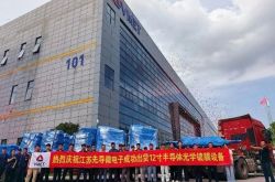
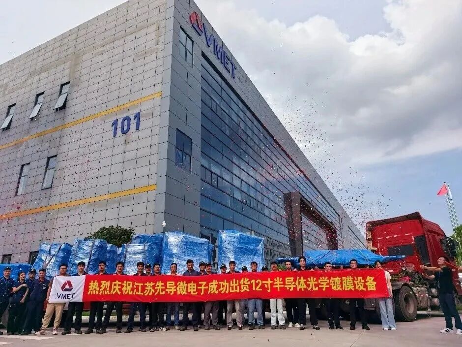
Lately, the premier Star600-EOSS 12-inch high-end precision optical magnetron sputtering system, independently engineered by Jiangsu LEAD Microelectronics, has undergone assembly, collaborative debugging, automation integration, and process validation at its production hub in the Xuzhou High-Tech Zone. This milestone achievement culminated in its formal handover to a premier domestic wafer manufacturing facility.
Tailored specifically for the large-scale production of 12-inch wafer optical coatings, this system employs a dual rotating cathode upward sputtering (Sputter-up) architecture to significantly minimize particle contamination. It achieves an impressive in-wafer film thickness uniformity of ≤±0.3%, coupled with exceptional wafer-to-wafer stability exceeding 0.3%. The system is adept at reliably supporting the mass production of intricate optical films, including infrared cut-off filters, AR anti-reflective coatings, optical waveguide dielectric films, and multi-layered narrowband filters (exceeding 100 layers), all without wavelength deviation and with assured production yields.
The system incorporates an in-situ wide-spectrum online monitoring mechanism, enabling real-time closed-loop adjustments to film thickness. It comes standard with an EFEM front-end module, seamlessly compatible with 12-inch FOUP wafer cassettes, and utilizes a vacuum robot for fully automated cassette-to-cassette material handling. Furthermore, it supports SECS/GEM and MES interconnections, facilitating continuous, unattended 7×24-hour production cycles. Its modular process design features multi-station independent magnetron cathodes, allowing for effortless switching between target materials. Optional enhancements include an ion source, plasma pretreatment capabilities, and a low-temperature temperature control platform, striking an optimal balance between R&D adaptability and mass production stability.
Drawing on the industrial chain strengths of its parent company, LEAD Tech Group, Jiangsu LEAD has forged a vertically integrated capability encompassing 'high-purity target material sourcing—coating equipment manufacturing—film process development.' Leveraging the group's optical target material resources, it can concurrently undertake target material matching and process formulation development for clients, offering comprehensive, tailored coating solutions.
This delivery signifies a pivotal transition for domestically produced high-end optical coating equipment, moving from technological parity to industrial implementation. It is poised to make sustained contributions to the high-quality advancement of the precision optics, wafer-level optics, and semiconductor sectors in the years ahead.
-
Financing and IPO: Is Ant Group a Financial Giant or a Pioneer in Cutting-Edge Tech?
-
![]()
Revenue Soars Twofold in Three Years! Optical Firm Reignites Bid for Hong Kong Stock Exchange Listing
-
![]()
Jiangsu LEAD Microelectronics Successfully Hands Over Its Inaugural 12-Inch Wafer-Level Optical Magnetron Sputtering System!
-
![]()
Domestic Computing Power Hits Breakthrough: Super Nodes as the Pivotal Force
-
![]()
Tongze Kangwei Secures IPO Registration on GEM: Broadband Terminal Equipment Provider Set for Imminent Share Issuance
-
![]()
Transforming Car Manufacturing into a 'Smartphone Launch' Frenzy: 5 Tips to Avoid Pitfalls When Purchasing a New Car
-
![]()
The Three-Way Battle Among AI Office Software: A Decade of War Among BAT
-
![]()
The Three-Way Battle Among AI Office Software: A Decade-Long War Among BAT