Domestic Triumph in Glass Substrate Lithography! Optical Firm Lands Major Orders
 10/16 2026
 388
388
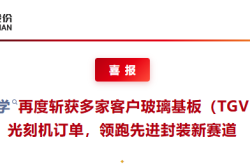
Recently, Honglei Optics, a subsidiary under the umbrella of Hongtian Co., Ltd., has clinched significant procurement contracts in the realm of glass substrate direct-write lithography. The company announced that its independently developed TGV glass substrate direct-write lithography equipment, along with direct-write lithography tools for semiconductor photomask applications, have been successfully delivered to customers.

The signing of these substantial contracts signifies Honglei Optics' transition from a 'trailblazing entrant' to a 'major order recipient' in the glass substrate direct-write lithography sector.
As a controlled subsidiary of Hongtian Co., Ltd., Honglei Optics concentrates on three key application domains: PCB HDI/FPC high-end circuit boards, semiconductor glass substrates (TGV), and advanced packaging photomasks. The company has set up R&D centers in both Shenzhen and Shanghai. According to Honglei Optics, all three of its micro-nano direct-write lithography equipment models have secured orders from top-tier industry clients.
The primary impetus for this market breakthrough stems from the replacement of traditional organic substrates with glass substrates in advanced packaging. With the swift rise of high-performance applications such as AI computing power chip packaging, CPO optical modules, and Micro LEDs, the wiring density and anti-warping capabilities of conventional organic substrates are nearing their thresholds.
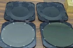
Industry specialists note that glass substrates leveraging TGV technology offer benefits like low electrical loss, high flatness, and anti-warping properties, rendering them ideal for next-generation packaging scenarios such as Chiplet heterogeneous integration and optoelectronic co-packaging. They are pivotal materials that underpin the ongoing advancement of AI computing power.
Glass substrates demonstrate a mere 0.3 dB/mm signal transmission loss at the 10 GHz frequency band, with dielectric loss slashed by over 50% compared to traditional organic substrates. TGV technology enables vertical interconnection between upper and lower layers by creating numerous micrometer-scale through-holes in the glass material and filling them with metal, thereby substantially shortening signal transmission paths and boosting interconnection density.
From an industry standpoint, numerous experts regard 2026 as a 'pivotal validation phase' for glass substrates, rather than the year of full-fledged mass production. The domestic TGV glass substrate sector is now at a critical juncture, transitioning from technical validation to small-scale mass production.
The industry generally anticipates that it will require an additional 2 to 3 years for key processes to mature, with the initial commercial adoption phase projected around 2028. Honglei Optics' accomplishment of delivering bulk orders at this juncture initially substantiates the mass production adaptability of its technical solutions for clients.
As the TGV process chain continues to mature and the demand for AI computing power chip packaging persists, the widespread adoption of domestic direct-write lithography equipment in this burgeoning sector indicates that the domestic supply chain for key advanced packaging equipment is gradually entering the industrialization adoption phase.
Whether Honglei Optics can leverage its first-mover advantage into sustained capacity delivery capabilities and process iteration capabilities will be the decisive factor in maintaining its competitiveness in this sector. OFweek Optics will keep a close eye on its subsequent market developments.
-
![]()
Thousand-Kilometer Range BMW i3, Ioniq V Priced Under RMB 100,000: Chinese Automakers Must Guard Against Joint Venture Encroachment in Global Expansion
-
![]()
Competition Among Cities Enters the Second Half: The Outcome Lies Beneath the Surface
-
![]()
AI-Generated Comic Drama Concept Stocks Surge: Is ByteDance the Sole Profit-Maker?
-
iPhone 18 Pro Series Sees Price Reductions—Apple Can't Afford to Stay Idle During Double 11
-
![]()
A Whopping 550 Million Yuan Investment! Fanchuangwei’s High-Transparency Optical AR Lens Project Takes Root in Taizhou
-
![]()
Domestic Triumph in Glass Substrate Lithography! Optical Firm Lands Major Orders
-
![]()
AI-Powered Alternatives Offer Free Substitutes, Posing Threat to Adobe's 'All-in-One' Suite
-
![]()
McKinsey Report: AI Inference to Account for 60% of Computing Power by 2030