Optical Waveguide Route Selection and Performance Optimization: Four Questions Integrators Must Answer Correctly
 10/09 2026
 423
423
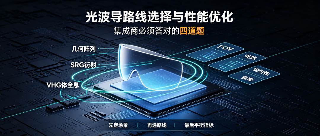
Abstract: By 2026, AR optical waveguides will transition from a single-route competition to a multi-route parallel approach involving geometric arrays, SRG, and VHG. SRG is set to deliver millions of units, VHG will launch production lines for millions of units, and geometric array production capacity will reach the million-unit level.
However, production line capability does not equate to stable terminal delivery. Rather than obsessing over parameters, selecting a route that aligns with product positioning is the core engineering decision for integrators.
By 2026, the AR optical waveguide industry will completely bid farewell to the 'single-route competition' and enter a new stage of mass production with multiple technology routes operating in parallel.
Geometric arrays will steadily land with flagship terminals, SRG diffraction will continue to expand production for large-scale delivery, and VHG volume holographic production lines will be concentrated and put into operation. The three routes will each fill the production capacity of their respective market segments but are still in a differentiated stage of 'production line formation and delivery ramp-up.'
However, for solution integrators and terminal product developers, the biggest misconception in the industry is obsessing over 'which technology route is stronger.'
The true industrial logic is the opposite: there is no best route, only the route that best fits the product positioning. Once the wrong route is chosen, all subsequent performance optimizations become ineffective iterations.
This article breaks down the underlying logic of optical waveguide route selection and the four key performance challenges that must be overcome for mass production.
01 Core of Route Selection: Define Product Scenarios Before Talking About Technology
Parameters such as geometric arrays, SRG diffraction, and VHG volume holography represent three distinct optical waveguide routes with entirely different physical principles, naturally corresponding to differentiated product positioning and commercial scenarios. There is no one-size-fits-all 'universal solution.'
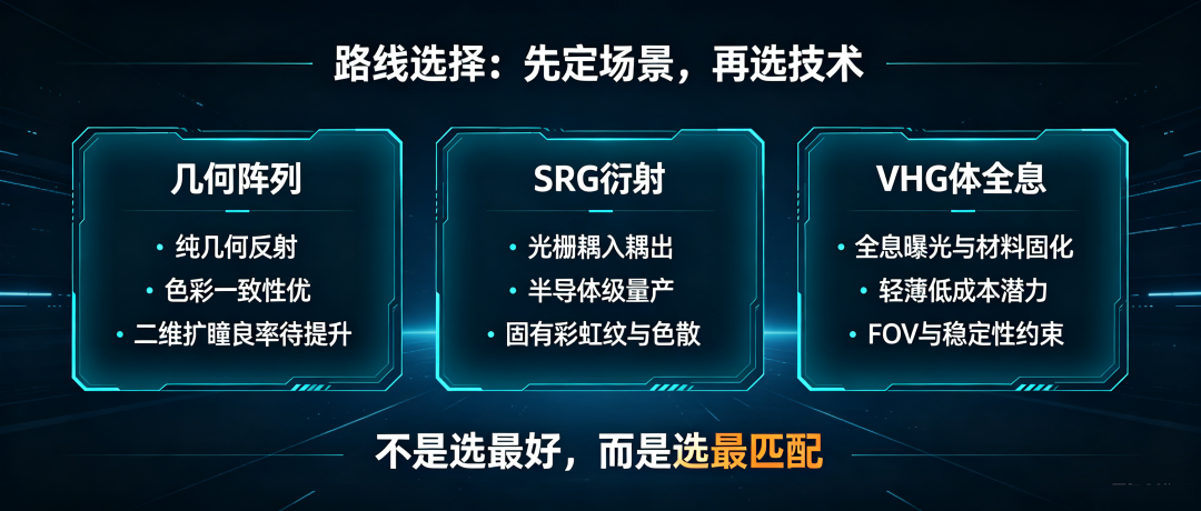
Geometric array optical waveguides rely on pure geometric reflection to transmit light beams, eliminating the need for nano-grating structures and fundamentally avoiding diffraction dispersion and rainbow artifacts. They offer the best color consistency and image purity among the three routes.
Their light leakage rate can be controlled within 5%, with one-dimensional array light efficiency utilization maintained at 5%–10%, making them ideally suited for high-end, full-color immersive display scenarios.
However, their process threshold (threshold) is extremely high, relying on precision cold processing, nano-coating, and molecular bonding technologies. Mass production yields for two-dimensional pupil expansion structures face significant bottlenecks.
SRG diffraction optical waveguides use grating structures for light beam coupling in and out, adaptable to semiconductor-grade mass production processes such as nano-imprinting and DUV lithography. They are currently the most industrially mature and easiest to scale up.
In the first half of 2026, over half of the 31 newly released AR glasses with optical waveguides adopted SRG solutions. However, their physical characteristics have inherent flaws, with rainbow artifacts and dispersion unable to be completely eliminated, only reduced by 30%–50% through process optimization.
VHG volume holographic optical waveguides do not require lithographic etching to prepare nano-grating structures, resulting in a relatively simplified process. Production relies on holographic exposure, material curing, precision coating, cutting, and packaging, yielding thin, transparent lenses with potential for low-cost mass production.
However, constrained by the refractive index system of photosensitive materials and environmental stability, mainstream products have a field of view (FOV) concentrated at 30°–40°, making them more suitable for entry-level, lightweight, and affordable consumer scenarios.
In short: choose geometric arrays for high-end, ultimate (ultimate) image quality; SRG for scalable mass production; and VHG for lightweight, economical products.
02 Four Must-Pass Challenges for Mass Production: FOV, Light Efficiency, Uniformity, and Yield
Once the technology route is determined, all product iterations and engineering optimizations revolve around four core indicators. These are the four key challenges integrators must overcome, directly determining product experience and commercialization capabilities.
FOV represents the physical performance ceiling of optical waveguides. The field of view for diffraction-based waveguides is constrained by grating period and substrate refractive index. Traditional glass substrates with a refractive index of 1.9–2.0 limit single-layer SRG FOV to within 40°.
High-refractive-index SiC materials can significantly broaden the optical K-domain, breaking through traditional material FOV limits. Meta Orion's prototype, relying on an SiC waveguide optical system, successfully demonstrated a 70°-class wide FOV experience.
However, whether single-layer planar SRG waveguides can stably achieve an ultra-wide 80° FOV depends on grating architecture, pupil expansion design, and precise matching with the entire optical engine, making it not yet a mature form for consumer-grade mass production in 2026.
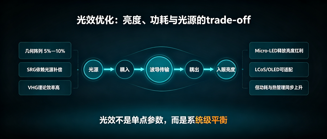
Light efficiency directly determines device brightness performance and overall power consumption.
Geometric array optical waveguides maintain stable light efficiency at 5%–10%. Conventional SRG light efficiency is relatively low but can fully leverage the performance advantages of Micro-LED high-brightness light sources. LCoS and OLED light sources can also adapt to SRG full-color schemes, though with relatively limited brightness benefits. VHG theoretically has natural advantages in diffraction efficiency but, constrained by photosensitive material systems and process limitations, has not yet fully unlocked its theoretical performance, leaving room for continuous optimization in mass production light efficiency.
Uniformity affects image perception. Energy decay during pupil expansion can lead to uneven brightness and dark bands in the image. Periodic grating structures can also cause imbalances in field of view and brightness uniformity, a common issue in full-color optical waveguides. Yield is the ultimate benchmark for technology implementation.
Industry leader AAC Technologies' SRG production line achieves stable mass production yields above 80% through full-process control, significantly outperforming the industry average of 50%. In contrast, geometrically arrayed optical waveguides, despite their performance advantages, still face widespread yield bottlenecks in two-dimensional pupil expansion.
03 FOV Optimization: The Triangular Trade-off Among Materials, Structures, and Design
Expanding the field of view is the most intuitive upgrade for user perception. The industry's mainstream optimization paths fall into three dimensions—materials, structures, and design—each with advantages and engineering trade-offs that cannot be fully balanced.
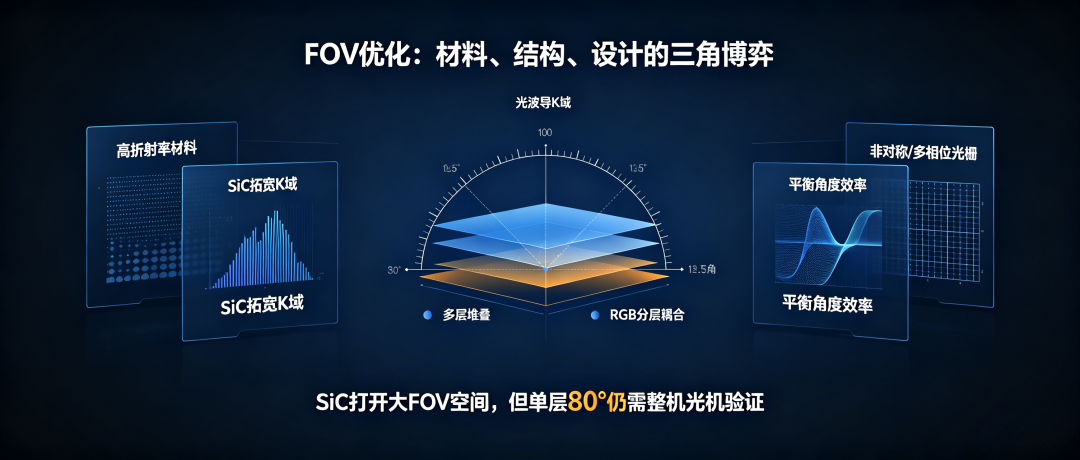
The material dimension focuses on upgrading to high-refractive-index substrates. Silicon carbide, with a refractive index exceeding 2.6, supports larger-angle light beam propagation, breaking through traditional glass FOV limits.
However, SiC materials are costly and brittle, making processing extremely difficult and unsuitable for affordable consumer products in the short term.
The structural dimension relies on multi-layer waveguide stacking, coupling RGB light beams into independent waveguide layers and optimizing diffraction efficiency for each wavelength.
The trade-off is doubled lens thickness and device weight, with extremely high alignment precision requirements for multi-layer bonding, significantly increasing mass production difficulty and defect rates.
The design dimension leverages asymmetric, multi-phase grating structures. By finely tuning grating tooth shape, duty cycle, and period parameters, diffraction efficiency for light beams at different incident angles can be balanced, pushing single-stage diffraction efficiency above 80% in specific bands and effectively improving edge field decay and brightness unevenness.
However, theoretical high grating efficiency does not directly equate to uniform full-color brightness across the entire eyebox. The final effect is still constrained by RGB coupling matching, eyebox range, and full-field pupil uniformity calibration.
04 Uniformity Optimization: Addressing Energy Imbalance in Pupil Expansion
The core cause of uneven optical waveguide images is energy decay during pupil expansion: light beams lose energy each time they pass through a coupling-out region, resulting in brighter images near the coupling-in point and darker images farther away, creating a noticeable brightness gradient. This is a common challenge for full-color optical waveguides.
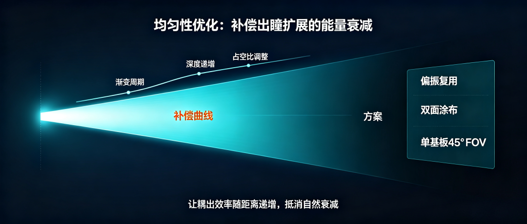
The industry's standard solution is gradient efficiency compensation: by designing gratings with gradually varying periods and dynamically adjusting grating depth and duty cycle along the propagation path, light beam coupling efficiency increases with propagation distance, offsetting natural energy decay and achieving uniform brightness across the entire field.
Academic research and industrial implementation have validated the optimization value of polarization multiplexing: through innovative processes like left- and right-hand circular polarization reuse and double-sided coating, energy decay can be effectively compensated while improving image uniformity and optical efficiency.
For example, Gudong Intelligence's single-layer PVG solution, relying on double-sided coating polarization multiplexing, achieves a 45° FOV with a single substrate, avoiding the thickness drawbacks of traditional dual-layer stacking and significantly reducing alignment deviations, thermal mismatch failures, and other mass production risks associated with multi-layer bonding.
05 Yield Breakthrough: From Manual Calibration to Wafer-Level Mass Production
Parameter optimization can only improve theoretical performance; yield improvements are essential for true scalable delivery. The mass production breakthrough for optical waveguides is fundamentally an upgrade in manufacturing systems.
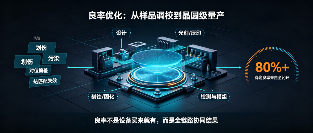
Goertek Optics' first domestic 12-inch DUV lithography etching mass production line reconstructs the optical waveguide production process to semiconductor-grade manufacturing standards. Leveraging high-precision overlay alignment, non-contact processing, and integrated multi-layer grating processes, it effectively avoids mass production (mass production) issues such as lens scratches, contamination, and alignment deviations, significantly improving product consistency and yield ceilings.
AAC Technologies' single-layer full-color SRG solution, relying on a closed-loop DUV lithography + etching process system, achieves an ultra-thin 0.7mm lens and ultra-light 4g weight, reducing weight by over 50% compared to traditional glass solutions while maintaining mass production yields above 80%.
The core gap in the industry lies not in equipment itself but in the collaborative capabilities across design, process, inspection, and module integration.
06 Optimal Solution for Integrators: Multi-Route Layout, Precise Matching by Scenario
The three optical waveguide routes each have strengths, weaknesses, and ceilings. No single route can dominate all scenarios. Leading integrators have reached a consensus: avoid betting on a single technology and instead adopt a multi-route parallel approach with scenario-specific implementations.
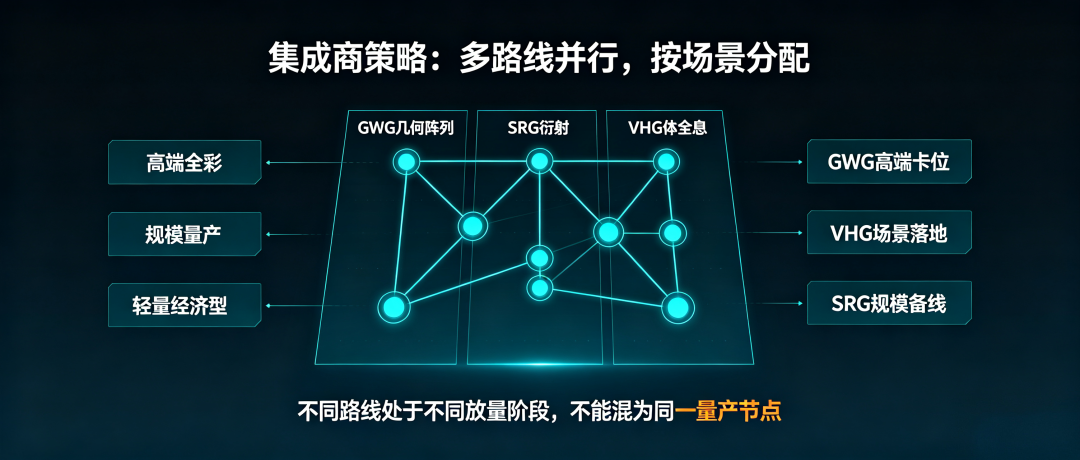
Crystal Optoelectronics' strategy is highly instructive: simultaneously developing GWG geometric arrays, VHG volume holography, and SRG diffraction across three routes to build a tiered AR optical product matrix.
In the high-end segment, it relies on GWG geometric arrays to achieve a 50° FOV, ultimate (ultimate) pure full-color image quality, and a 1.3mm ultra-thin lens certified by leading clients, securing deep cooperation with North American enterprises. Currently in client validation and pilot production ramp-up. For the mid-range lightweight market, it deploys VHG volume holography, with one-dimensional pupil expansion products already in small-batch production and two-dimensional pupil expansion schemes under continuous iterative development. Simultaneously, it advances glass and SiC dual-wafer SRG production line layouts, steadily upgrading to 12-inch large-scale mass production.
For Crystal Optoelectronics, the three routes serve distinct purposes: high-end positioning, scenario-specific implementation, and scalable backup, each at a different stage of volume ramp-up and not synchronously mature as equivalent mass production solutions.
In Conclusion
Route selection and performance optimization for AR optical waveguides are never a single-technology question but an engineering decision-making challenge under multiple constraints. There is no perfect technology route, only the optimal solution for a given scenario.
The four key challenges—FOV, light efficiency, uniformity, and yield—cannot all be perfected simultaneously. The core competitiveness of integrators lies in finding the best balance among performance, cost, and manufacturability based on their product positioning.
Only with the right technology route can all performance optimizations hold value. With the correct direction, even slow iterations represent progress; with a misaligned route, all efforts become wasted energy.
Interactive Topic: The four core challenges for AR optical waveguide mass production are FOV, light efficiency, uniformity, and yield. If product iteration could only prioritize one indicator, would you choose wide FOV, high light efficiency, high uniformity, or high yield? Welcome to share your product decision-making logic in the comments.
— AR Andy | Focusing on optical waveguides and AR microdisplay tracks, deeply dissecting the underlying logic of the optics industry
[Risk Disclaimer] This article is based on publicly disclosed corporate information and industry data, serving only as industrial insights and technical popularization of science (popularization). Processes and metrics vary among manufacturers and do not constitute technical selection or investment advice.
-
![]()
What is the boundary of collaboration between FAW Toyota and GAC Toyota behind FAW Toyota's 'independent survival'?
-
![]()
Optical Waveguide Route Selection and Performance Optimization: Four Questions Integrators Must Answer Correctly
-
![]()
The Collective Surge of Major AI Models Toward Public Listing: The High-Stakes Race Behind the Buzz
-
![]()
A Staggering $50 Billion Valuation! The Resurgence of a Tsinghua-Educated Engineer’s Venture
-
![]()
In His Inaugural Year, Porsche CEO Implements Three Daring Strategies: 9,000 Job Cuts, 20% Price Increase, and Reintroduction of Gasoline Cars
-
![]()
JAC’s Stock Plummets to Limit Down! Dcd Auto Tests Zunjie V800, Three Consecutive Cars Experience Brake Failures: Extreme Testing or Defective Product? | Mingjingpro
-
![]()
【Electric Equipment】Fengcheng Zhuoxin Logistics Signs Contract for 150 SANY Electric Heavy Trucks
-
![]()
[Intelligentization] Huawei and Seres Sign New Five-Year Cooperation